- 您现在的位置:买卖IC网 > PDF目录9924 > IDT723673L15PF (IDT, Integrated Device Technology Inc)IC FIFO SYNC 8192X36 128QFP PDF资料下载
参数资料
| 型号: | IDT723673L15PF |
| 厂商: | IDT, Integrated Device Technology Inc |
| 文件页数: | 24/29页 |
| 文件大小: | 0K |
| 描述: | IC FIFO SYNC 8192X36 128QFP |
| 标准包装: | 36 |
| 系列: | 7200 |
| 功能: | 同步 |
| 存储容量: | 288K(8K x 36) |
| 数据速率: | 67MHz |
| 访问时间: | 15ns |
| 电源电压: | 4.5 V ~ 5.5 V |
| 工作温度: | 0°C ~ 70°C |
| 安装类型: | 表面贴装 |
| 封装/外壳: | 128-LQFP |
| 供应商设备封装: | 128-TQFP(14x20) |
| 包装: | 托盘 |
| 其它名称: | 723673L15PF |
第1页第2页第3页第4页第5页第6页第7页第8页第9页第10页第11页第12页第13页第14页第15页第16页第17页第18页第19页第20页第21页第22页第23页当前第24页第25页第26页第27页第28页第29页
4
COMMERCIALTEMPERATURERANGE
IDT723653/723663/723673 CMOS SyncFIFOTM WITH BUS-MATCHING
2,048 x 36 x 2, 4,096 x 36 x 2 and 8,192 x 36 x 2
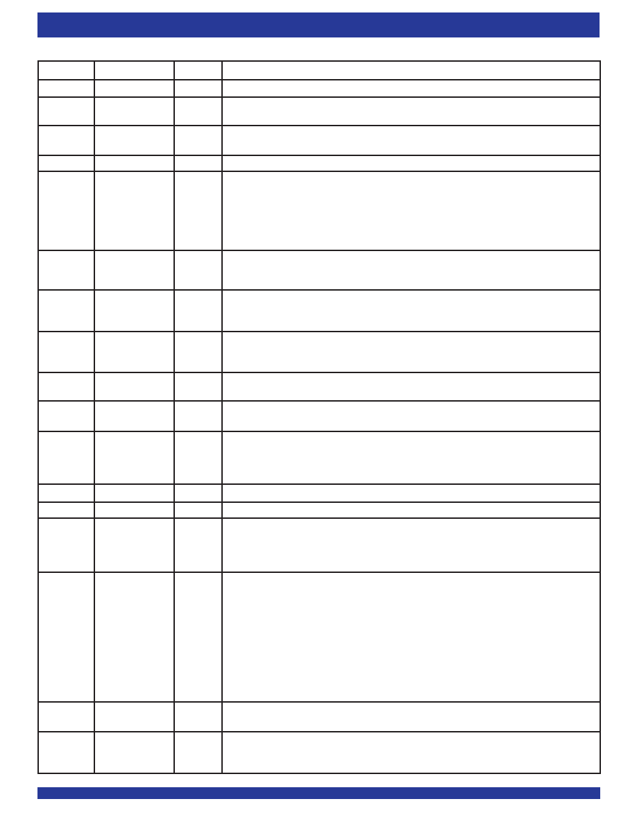
PIN DESCRIPTIONS
Symbol
Name
I/O
Description
A0-A35
Port A Data
I/O
36-bit bidirectional data port for side A.
AE
Almost-EmptyFlag
O
Programmable Almost-Empty flag synchronized to CLKB. It is LOW when the number of words in the
(Port B)
FIFO is less than or equal to the value in the Almost-Empty B offset register, X.
AF
Almost-FullFlag
O
Programmable Almost-Full flag synchronized to CLKA. It is LOW when the number of empty
(Port A)
locations in the FIFO is less than or equal to the value in the Almost-Full A offset register, Y.
B0-B35
Port B Data
I/O
36-bit bidirectional data port for side B.
BE/
FWFT
Big-Endian/
I
This is a dual purpose pin. During Master Reset, a HIGH on BE will select Big-Endian operation. In
First Word
this case, depending on the bus size, the most significant byte or word written to Port A is read from
Fall Through
Port B first. A LOW on BE will select Little-Endian operation. In this case, the least significant byte or
word written to Port A is read from Port B first. After Master Reset, this pin selects the timing mode. A
HIGH on
FWFT selects IDT Standard mode, a LOW selects First Word Fall Through mode. Once
the timing mode has been selected, the level on
FWFT must be static throughout device operation.
BM(1)
Bus-MatchSelect
I
A HIGH on this pin enables either byte or word bus width on Port B, depending on the state of
(Port B)
SIZE. A LOW selects long word operation. BM works with SIZE and BE to select the bus size and
endian arrangement for Port B.The level of BM must be static throughout device operation.
CLKA
Port A Clock
I
CLKA is a continuous clock that synchronizes all data transfers through Port A and can be
asynchronous or coincident to CLKB.
FF/IR and AF are synchronized to the LOW-to-HIGH
transition of CLKA.
CLKB
Port B Clock
I
CLKB is a continuous clock that synchronizes all data transfers through Port B and can be
asynchronous or coincident to CLKA.
EF/OR and AE are synchronized to the LOW-to-HIGH
transition of CLKB.
CSA
Port A Chip
I
CSA must be LOW to enable to LOW-to-HIGH transition of CLKA to read or write on Port A.The
Select
A0-A35 outputs are in the high-impedance state when
CSA is HIGH.
CSB
Port B Chip
I
CSB must be LOW to enable a LOW-to-HIGH transition of CLKB to read or write data on Port B.
Select
The B0-B35 outputs are in the high-impedance state when
CSB is HIGH.
EF/OR
Empty/Output
O
This is a dual function pin. In the IDT Standard mode, the
EF function is selected. EFindicates
Ready Flag
whether or not the FIFO memory is empty. In the FWFT mode, the OR function is selected. OR indicates
(Port B)
the presence of valid data on the B0-B35 outputs, available for reading.
EF/OR is synchronized to the
LOW-to-HIGH transition of CLKB.
ENA
Port A Enable
I
ENA must be HIGH to enable a LOW-to-HIGH transition of CLKA to read or write data on Port A.
ENB
Port B Enable
I
ENB must be HIGH to enable a LOW-to-HIGH transition of CLKB to read or write data on Port B.
FF/IR
Full/Input
O
This is a dual function pin. In the IDT Standard mode, the
FF function is selected. FF indicates
Ready Flag
whether or not the FIFO memory is full. In the FWFT mode, the IR function is selected. IR indicates
(Port A)
whether or not there is space available for writing to the FIFO memory.
FF/IR is synchronized to the
LOW-to-HIGH transition of CLKA.
FS0/SD
Flag Offset Select 0/
I
FS1/
SEN and FS0/SD are dual-purpose inputs used for flag offset register programming. During
Serial Data,
Reset, FS1/
SENandFS0/SD,togetherwithFS2selecttheflagoffsetprogrammingmethod. Three
offset register programming methods are available: automatically load one of five preset values (8,
16, 64, 256 or 1,024), parallel load from Port A, and serial load.
FS1/
SEN
Flag Offset Select 1/
I
Serial Enable
When serial load is selected for flag offset register programming, FS1/
SEN is used as an enable
synchronous to the LOW-to-HIGH transition of CLKA. When FS1/
SEN is LOW, a rising edge on
FS2(1)
Flag Offset Select 2
I
CLKA load the bit present on FS0/SD into the X and Y registers. The number of bit writes required
to program the offset registers is 22 for the IDT723653, 24 for the IDT723663, and 26 for the IDT723673.
The first bit write stores the Y-register MSB and the last bit write stores the X-register LSB.
MBA
Port A Mailbox
I
A HIGH level on MBA chooses a mailbox register for a Port A read or write operation.
Select
MBB
Port B Mailbox
I
A HIGH level on MBB chooses a mailbox register for a Port B read or write operation. When the
Select
B0-B35 outputs are active, a HIGH level on MBB selects data from the mail1 register for output and
a LOW level selects FIFO data for output.
相关PDF资料 |
PDF描述 |
|---|---|
| MX7576KP+T | IC ADC 8BIT MPU COMP 20-PLCC |
| IDT72V293L7-5PF8 | IC FIFO 65536X18 7-5NS 80QFP |
| ICL3232ECBNZ-T7A | IC TXRX RS232 DUAL ESD 16SOIC |
| MAX166DCPP+ | IC ADC 8BIT MPU COMP 20-DIP |
| IDT72V293L10PFI8 | IC FIFO 65536X18 10NS 80QFP |
相关代理商/技术参数 |
参数描述 |
|---|---|
| IDT723673L15PF8 | 功能描述:IC FIFO SYNC 8192X36 128QFP RoHS:否 类别:集成电路 (IC) >> 逻辑 - FIFO 系列:7200 标准包装:15 系列:74F 功能:异步 存储容量:256(64 x 4) 数据速率:- 访问时间:- 电源电压:4.5 V ~ 5.5 V 工作温度:0°C ~ 70°C 安装类型:通孔 封装/外壳:24-DIP(0.300",7.62mm) 供应商设备封装:24-PDIP 包装:管件 其它名称:74F433 |
| IDT723674L12PF | 功能描述:IC FIFO SYNC 16384X36 128QFP RoHS:否 类别:集成电路 (IC) >> 逻辑 - FIFO 系列:7200 标准包装:15 系列:74F 功能:异步 存储容量:256(64 x 4) 数据速率:- 访问时间:- 电源电压:4.5 V ~ 5.5 V 工作温度:0°C ~ 70°C 安装类型:通孔 封装/外壳:24-DIP(0.300",7.62mm) 供应商设备封装:24-PDIP 包装:管件 其它名称:74F433 |
| IDT723674L12PF8 | 功能描述:IC FIFO SYNC 16384X36 128QFP RoHS:否 类别:集成电路 (IC) >> 逻辑 - FIFO 系列:7200 标准包装:15 系列:74F 功能:异步 存储容量:256(64 x 4) 数据速率:- 访问时间:- 电源电压:4.5 V ~ 5.5 V 工作温度:0°C ~ 70°C 安装类型:通孔 封装/外壳:24-DIP(0.300",7.62mm) 供应商设备封装:24-PDIP 包装:管件 其它名称:74F433 |
| IDT723674L15PF | 功能描述:IC FIFO SYNC 16384X36 128QFP RoHS:否 类别:集成电路 (IC) >> 逻辑 - FIFO 系列:7200 标准包装:15 系列:74F 功能:异步 存储容量:256(64 x 4) 数据速率:- 访问时间:- 电源电压:4.5 V ~ 5.5 V 工作温度:0°C ~ 70°C 安装类型:通孔 封装/外壳:24-DIP(0.300",7.62mm) 供应商设备封装:24-PDIP 包装:管件 其它名称:74F433 |
| IDT723674L15PF8 | 功能描述:IC FIFO SYNC 16384X36 128QFP RoHS:否 类别:集成电路 (IC) >> 逻辑 - FIFO 系列:7200 标准包装:15 系列:74F 功能:异步 存储容量:256(64 x 4) 数据速率:- 访问时间:- 电源电压:4.5 V ~ 5.5 V 工作温度:0°C ~ 70°C 安装类型:通孔 封装/外壳:24-DIP(0.300",7.62mm) 供应商设备封装:24-PDIP 包装:管件 其它名称:74F433 |
发布紧急采购,3分钟左右您将得到回复。