- 您现在的位置:买卖IC网 > PDF目录10009 > IDT72V3612L20PQF (IDT, Integrated Device Technology Inc)IC FIFO 64X36X2 20NS 132QFP PDF资料下载
参数资料
| 型号: | IDT72V3612L20PQF |
| 厂商: | IDT, Integrated Device Technology Inc |
| 文件页数: | 19/24页 |
| 文件大小: | 0K |
| 描述: | IC FIFO 64X36X2 20NS 132QFP |
| 标准包装: | 36 |
| 系列: | 72V |
| 功能: | 异步 |
| 存储容量: | 4.6K(64 x 36 x2) |
| 数据速率: | 50MHz |
| 访问时间: | 20ns |
| 电源电压: | 3 V ~ 3.6 V |
| 工作温度: | 0°C ~ 70°C |
| 安装类型: | 表面贴装 |
| 封装/外壳: | 132-BQFP 缓冲式 |
| 供应商设备封装: | 132-PQFP(24.13x24.13) |
| 包装: | 托盘 |
| 其它名称: | 72V3612L20PQF |
4
IDT72V3612 3.3V, CMOS SyncBiFIFOTM
64 x 36 x 2
COMMERCIALTEMPERATURERANGE
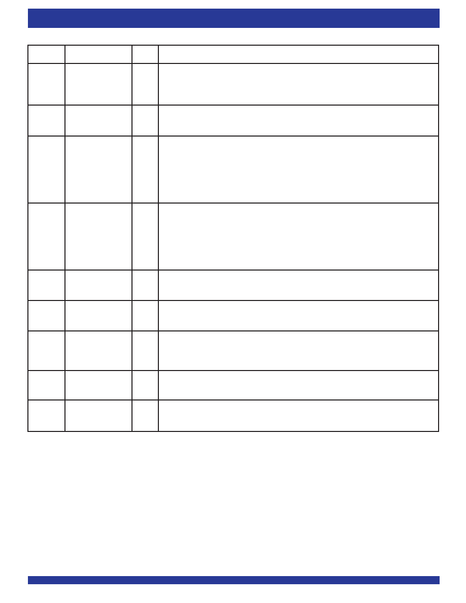
PIN DESCRIPTION (CONTINUED)
Symbol
Name
I/O
Description
MBF2
Mail2 Register Flag
O
MBF2 is set LOW by a LOW-to-HIGH transition of CLKB that writes data to the mail2 register.
Writes to the mail2 register are inhibited while MBF2 is set LOW. MBF2 is set HIGH by a LOW-to-
HIGH transition of CLKA when a port A read is selected and MBA is HIGH. MBF2 is set HIGH
when the device is reset.
ODD/
Odd/Even Parity
I
Odd parity is checked on each port when ODD/EVEN is HIGH, and even parity is checked when
EVEN
Select
ODD/EVEN is LOW. ODD/EVEN also selects the type of parity generated for each port if parity
generation is enabled for a read operation.
PEFA
Port A Parity Error
O
When any byte applied to terminals A0-A35 fails parity, PEFA is LOW. Bytes are organized as
Flag
(Port A)
A0-A8, A9-A17, A18-A26, and A27-A35, with the most significant bit of each byte serving as the
parity bit. The type of parity checked is determined by the state of the ODD/EVEN input. The
parity trees used to check the A0-A35 inputs are shared by the mail2 register to generate parity if
parity generation is selected by PGA. Therefore, if a mail2 read with parity generation is setup by
having W/RA LOW, MBA HIGH, and PGA HIGH, the PEFA flag is forced HIGH regardless of the
A0-A35 inputs.
PEFB
Port B Parity Error
O
When any byte applied to terminals B0-B35 fails parity, PEFB is LOW. Bytes are organized as
Flag
(Port B)
B0-B8, B9-B17, B18-B26, B27-B35 with the most significant bit of each byte serving as the parity
bit. The type of parity checked is determined by the state of the ODD/EVEN input. The parity trees
used to check the B0-B35 inputs are shared by the mail1 register to generate parity if parity
generation is selected by PGB. Therefore, if a mail1 read with parity generation is setup by having
W/RB LOW, MBB HIGH, and PGB HIGH, the PEFB flag is forced HIGH regardless of the state of
the B0-B35 inputs.
PGA
Port A Parity
I
Parity is generated for data reads from port A when PGA is HIGH. The type of parity generated is
Generation
selected by the state of the ODD/EVEN input. Bytes are organized as A0-A8, A9-A17, A18-A26,
and A27-A35. The generated parity bits are output in the most significant bit of each byte.
PGB
Port B Parity
I
Parity is generated for data reads from port B when PGB is HIGH. The type of parity generated is
Generation
selected by the state of the ODD/EVEN input. Bytes are organized as B0-B8, B9-B17, B18-B26,
and B27-B35. The generated parity bits are output in the most significant bit of each byte.
RST
Reset
I
To reset the device, four LOW-to-HIGH transitions of CLKA and four LOW-to-HIGH transitions of
CLKB must occur while RST is LOW. This sets the AFA, AFB, MBF1, and MBF2 flags HIGH and
the EFA, EFB, AEA, AEB, FFA, and FFB flags LOW. The LOW-to-HIGH transition of RST latches
the status of the FS1 and FS0 inputs to select Almost-Full and Almost-Empty flag offset.
W/RA
Port A Write/Read
I
A HIGH selects a write operation and a LOW selects a read operation on port A for a LOW-to-
Select
HIGH transition of CLKA. The A0-A35 outputs are in the high-impedance state when W/RA is
HIGH.
W/RB
Port B Write/Read
I
A HIGH selects a write operation and a LOW selects a read operation on port B for a LOW-to-
Select
HIGH transition of CLKB. The B0-B35 outputs are in the high-impedance state when W/RB is
HIGH.
相关PDF资料 |
PDF描述 |
|---|---|
| VI-B1B-MW | CONVERTER MOD DC/DC 95V 100W |
| VI-263-IX-B1 | CONVERTER MOD DC/DC 24V 75W |
| IDT72V3611L20PQF | IC FIFO SYNC 64X36 20NS 132-PQFP |
| VI-263-IW-F4 | CONVERTER MOD DC/DC 24V 100W |
| IDT72V3614L20PF | IC FIFO 64X36X2 20NS 120QFP |
相关代理商/技术参数 |
参数描述 |
|---|---|
| IDT72V3613L12PF | 功能描述:IC FIFO CLOCK 64X36 12NS 120TQFP RoHS:否 类别:集成电路 (IC) >> 逻辑 - FIFO 系列:72V 标准包装:90 系列:7200 功能:同步 存储容量:288K(16K x 18) 数据速率:100MHz 访问时间:10ns 电源电压:4.5 V ~ 5.5 V 工作温度:0°C ~ 70°C 安装类型:表面贴装 封装/外壳:64-LQFP 供应商设备封装:64-TQFP(14x14) 包装:托盘 其它名称:72271LA10PF |
| IDT72V3613L12PF8 | 功能描述:IC FIFO CLOCK 64X36 12NS 120TQFP RoHS:否 类别:集成电路 (IC) >> 逻辑 - FIFO 系列:72V 标准包装:90 系列:7200 功能:同步 存储容量:288K(16K x 18) 数据速率:100MHz 访问时间:10ns 电源电压:4.5 V ~ 5.5 V 工作温度:0°C ~ 70°C 安装类型:表面贴装 封装/外壳:64-LQFP 供应商设备封装:64-TQFP(14x14) 包装:托盘 其它名称:72271LA10PF |
| IDT72V3613L12PQF | 功能描述:IC FIFO CLOCK 64X36 12NS 132PQFP RoHS:否 类别:集成电路 (IC) >> 逻辑 - FIFO 系列:72V 标准包装:90 系列:7200 功能:同步 存储容量:288K(16K x 18) 数据速率:100MHz 访问时间:10ns 电源电压:4.5 V ~ 5.5 V 工作温度:0°C ~ 70°C 安装类型:表面贴装 封装/外壳:64-LQFP 供应商设备封装:64-TQFP(14x14) 包装:托盘 其它名称:72271LA10PF |
| IDT72V3613L15PF | 功能描述:IC FIFO CLOCK 64X36 15NS 120TQFP RoHS:否 类别:集成电路 (IC) >> 逻辑 - FIFO 系列:72V 标准包装:90 系列:7200 功能:同步 存储容量:288K(16K x 18) 数据速率:100MHz 访问时间:10ns 电源电压:4.5 V ~ 5.5 V 工作温度:0°C ~ 70°C 安装类型:表面贴装 封装/外壳:64-LQFP 供应商设备封装:64-TQFP(14x14) 包装:托盘 其它名称:72271LA10PF |
| IDT72V3613L15PF8 | 功能描述:IC FIFO CLOCK 64X36 15NS 120TQFP RoHS:否 类别:集成电路 (IC) >> 逻辑 - FIFO 系列:72V 标准包装:90 系列:7200 功能:同步 存储容量:288K(16K x 18) 数据速率:100MHz 访问时间:10ns 电源电压:4.5 V ~ 5.5 V 工作温度:0°C ~ 70°C 安装类型:表面贴装 封装/外壳:64-LQFP 供应商设备封装:64-TQFP(14x14) 包装:托盘 其它名称:72271LA10PF |
发布紧急采购,3分钟左右您将得到回复。