- 您现在的位置:买卖IC网 > PDF目录9949 > IDT72V3680L10PF8 (IDT, Integrated Device Technology Inc)IC FIFO SS 16384X36 10NS 128TQFP PDF资料下载
参数资料
| 型号: | IDT72V3680L10PF8 |
| 厂商: | IDT, Integrated Device Technology Inc |
| 文件页数: | 40/46页 |
| 文件大小: | 0K |
| 描述: | IC FIFO SS 16384X36 10NS 128TQFP |
| 标准包装: | 1,000 |
| 系列: | 72V |
| 功能: | 异步,同步 |
| 存储容量: | 576K(16K x 36) |
| 数据速率: | 100MHz |
| 访问时间: | 10ns |
| 电源电压: | 3.15 V ~ 3.45 V |
| 工作温度: | 0°C ~ 70°C |
| 安装类型: | 表面贴装 |
| 封装/外壳: | 128-LQFP |
| 供应商设备封装: | 128-TQFP(14x20) |
| 包装: | 带卷 (TR) |
| 其它名称: | 72V3680L10PF8 |
第1页第2页第3页第4页第5页第6页第7页第8页第9页第10页第11页第12页第13页第14页第15页第16页第17页第18页第19页第20页第21页第22页第23页第24页第25页第26页第27页第28页第29页第30页第31页第32页第33页第34页第35页第36页第37页第38页第39页当前第40页第41页第42页第43页第44页第45页第46页
45
COMMERCIAL AND INDUSTRIAL
TEMPERATURE RANGES
IDT72V3640/50/60/70/80/90 3.3V HIGH DENSITY SUPERSYNC IITM 36-BIT FIFO
1,024 x 36, 2,048 x 36, 4,096 x 36, 8,192 x 36, 16,384 x 36 and 32,768 x 36
OCTOBER 22, 2008
THE INSTRUCTION REGISTER
TheInstructionregisterallowsaninstructiontobeshiftedinseriallyintothe
processor at the rising edge of TCLK.
The Instruction is used to select the test to be performed, or the test data
registertobeaccessed,orboth. Theinstructionshiftedintotheregisterislatched
at the completion of the shifting process when the TAP controller is at Update-
IRstate.
The instruction register must contain 4 bit instruction register-based cells
whichcanholdinstructiondata. Thesemandatorycellsarelocatednearestthe
serial outputs they are the least significant bits.
TEST DATA REGISTER
The Test Data register contains three test data registers: the Bypass, the
Boundary Scan register and Device ID register.
These registers are connected in parallel between a common serial input
and a common serial data output.
The following sections provide a brief description of each element. For a
completedescription,refertotheIEEEStandardTestAccessPortSpecification
(IEEE Std. 1149.1-1990).
TEST BYPASS REGISTER
The register is used to allow test data to flow through the device from TDI
toTDO. Itcontainsasinglestageshiftregisterforaminimumlengthinserialpath.
When the bypass register is selected by an instruction, the shift register stage
is set to a logic zero on the rising edge of TCLK when the TAP controller is in
the Capture-DR state.
The operation of the bypass register should not have any effect on the
operation of the device in response to the BYPASS instruction.
THE BOUNDARY-SCAN REGISTER
The Boundary Scan Register allows serial data TDI be loaded in to or read
out of the processor input/output ports. The Boundary Scan Register is a part
of the IEEE 1149.1-1990 Standard JTAG Implementation.
THE DEVICE IDENTIFICATION REGISTER
The Device Identification Register is a Read Only 32-bit register used to
specify the manufacturer, part number and version of the processor to be
determined through the TAP in response to the IDCODE instruction.
IDT JEDEC ID number is 0xB3. This translates to 0x33 when the parity
is dropped in the 11-bit Manufacturer ID field.
For the IDT72V3640/72V3650/72V3660/72V3670/72V3680/72V3690,
the Part Number field contains the following values:
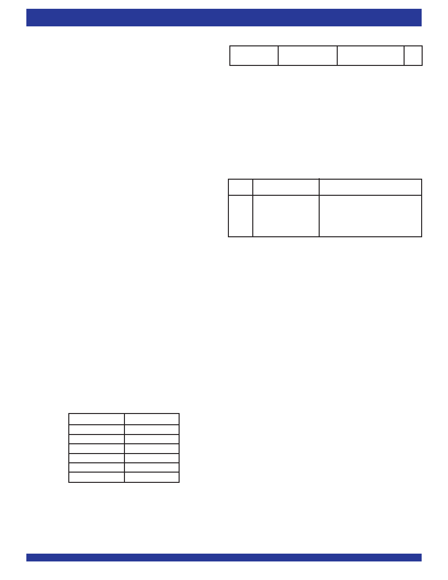
IDT72V3640/50/60/70/80/90 JTAG Device Identification Register
31(MSB)
28 27
12 11
1 0(LSB)
Version (4 bits)
Part Number (16-bit) Manufacturer ID (11-bit)
0X0
0X33
1
JTAG INSTRUCTION REGISTER
TheInstructionregisterallowsinstructiontobeseriallyinputintothedevice
when the TAP controller is in the Shift-IR state. The instruction is decoded to
perform the following:
Select test data registers that may operate while the instruction is
current. The other test data registers should not interfere with chip
operation and the selected data register.
Definetheserialtestdataregisterpaththatisusedtoshiftdatabetween
TDI and TDO during data register scanning.
The Instruction Register is a 4 bit field (i.e.IR3, IR2, IR1, IR0) to decode 16
different possible instructions. Instructions are decoded as follows.
Hex
Instruction
Function
Value
0x00
EXTEST
Select Boundary Scan Register
0x02
IDCODE
Select Chip Identification data register
0x01
SAMPLE/PRELOAD
Select Boundary Scan Register
0x03
HI-Z
JTAG
0x0F
BYPASS
Select Bypass Register
Table 6. JTAG Instruction Register Decoding
The following sections provide a brief description of each instruction. For
acompletedescriptionrefertotheIEEEStandardTestAccessPortSpecification
(IEEE Std. 1149.1-1990).
EXTEST
The mandatory EXTEST instruction is provided for external circuity and
board level interconnection check.
IDCODE
This instruction is provided to select Device Identification Register to read
out manufacture’s identity, part number and version number.
SAMPLE/PRELOAD
The mandatory SAMPLE/PRELOAD instruction allows data values to be
loadedontothelatchedparalleloutputsoftheboundary-scanshiftregisterprior
to selection of the boundary-scan test instruction. The SAMPLE instruction
allowsasnapshotofdataflowingfromthesystempinstotheon-chiplogicorvice
versa.
HIGH-Z
Thisinstructionplacesalltheoutputpinsonthedeviceintoahighimpedance
state.
BYPASS
The Bypass instruction contains a single shift-register stage and is set to
provide a minimum-length serial path between the TDI and the TDO pins of the
device when no test operation of the device is required.
Device
Part# Field
IDT72V3640
04E5
IDT72V3650
04E4
IDT72V3660
04E3
IDT72V3670
04E2
IDT72V3680
04E1
IDT72V3690
04E0
相关PDF资料 |
PDF描述 |
|---|---|
| MS27468T11B35S EDR | CONN RCPT 13POS JAM NUT W/SCKT |
| IDT72V3676L15PF8 | IC FIFO 16384X36 15NS 128QFP |
| MS3120P14-18S | CONN RCPT 18POS WALL MNT W/SCKT |
| IDT72V3674L15PF8 | IC FIFO 16384X36 15NS 128QFP |
| MS27467T11B35P EDR | CONN PLUG 13POS STRAIGHT W/PINS |
相关代理商/技术参数 |
参数描述 |
|---|---|
| IDT72V3680L10PFI | 制造商:Integrated Device Technology Inc 功能描述: |
| IDT72V3680L15PF | 功能描述:IC FIFO SS 16384X36 15NS 128TQFP RoHS:否 类别:集成电路 (IC) >> 逻辑 - FIFO 系列:72V 标准包装:15 系列:74F 功能:异步 存储容量:256(64 x 4) 数据速率:- 访问时间:- 电源电压:4.5 V ~ 5.5 V 工作温度:0°C ~ 70°C 安装类型:通孔 封装/外壳:24-DIP(0.300",7.62mm) 供应商设备封装:24-PDIP 包装:管件 其它名称:74F433 |
| IDT72V3680L15PF8 | 功能描述:IC FIFO SS 16384X36 15NS 128TQFP RoHS:否 类别:集成电路 (IC) >> 逻辑 - FIFO 系列:72V 标准包装:15 系列:74F 功能:异步 存储容量:256(64 x 4) 数据速率:- 访问时间:- 电源电压:4.5 V ~ 5.5 V 工作温度:0°C ~ 70°C 安装类型:通孔 封装/外壳:24-DIP(0.300",7.62mm) 供应商设备封装:24-PDIP 包装:管件 其它名称:74F433 |
| IDT72V3680L15PFI | 功能描述:IC FIFO SS 16384X36 15NS 128TQFP RoHS:否 类别:集成电路 (IC) >> 逻辑 - FIFO 系列:72V 标准包装:15 系列:74F 功能:异步 存储容量:256(64 x 4) 数据速率:- 访问时间:- 电源电压:4.5 V ~ 5.5 V 工作温度:0°C ~ 70°C 安装类型:通孔 封装/外壳:24-DIP(0.300",7.62mm) 供应商设备封装:24-PDIP 包装:管件 其它名称:74F433 |
| IDT72V3680L15PFI8 | 功能描述:IC FIFO SS 16384X36 15NS 128TQFP RoHS:否 类别:集成电路 (IC) >> 逻辑 - FIFO 系列:72V 标准包装:15 系列:74F 功能:异步 存储容量:256(64 x 4) 数据速率:- 访问时间:- 电源电压:4.5 V ~ 5.5 V 工作温度:0°C ~ 70°C 安装类型:通孔 封装/外壳:24-DIP(0.300",7.62mm) 供应商设备封装:24-PDIP 包装:管件 其它名称:74F433 |
发布紧急采购,3分钟左右您将得到回复。