- 您现在的位置:买卖IC网 > PDF目录9949 > IDT72V3680L10PF8 (IDT, Integrated Device Technology Inc)IC FIFO SS 16384X36 10NS 128TQFP PDF资料下载
参数资料
| 型号: | IDT72V3680L10PF8 |
| 厂商: | IDT, Integrated Device Technology Inc |
| 文件页数: | 44/46页 |
| 文件大小: | 0K |
| 描述: | IC FIFO SS 16384X36 10NS 128TQFP |
| 标准包装: | 1,000 |
| 系列: | 72V |
| 功能: | 异步,同步 |
| 存储容量: | 576K(16K x 36) |
| 数据速率: | 100MHz |
| 访问时间: | 10ns |
| 电源电压: | 3.15 V ~ 3.45 V |
| 工作温度: | 0°C ~ 70°C |
| 安装类型: | 表面贴装 |
| 封装/外壳: | 128-LQFP |
| 供应商设备封装: | 128-TQFP(14x20) |
| 包装: | 带卷 (TR) |
| 其它名称: | 72V3680L10PF8 |
第1页第2页第3页第4页第5页第6页第7页第8页第9页第10页第11页第12页第13页第14页第15页第16页第17页第18页第19页第20页第21页第22页第23页第24页第25页第26页第27页第28页第29页第30页第31页第32页第33页第34页第35页第36页第37页第38页第39页第40页第41页第42页第43页当前第44页第45页第46页
7
COMMERCIAL AND INDUSTRIAL
TEMPERATURE RANGES
IDT72V3640/50/60/70/80/90 3.3V HIGH DENSITY SUPERSYNC IITM 36-BIT FIFO
1,024 x 36, 2,048 x 36, 4,096 x 36, 8,192 x 36, 16,384 x 36 and 32,768 x 36
OCTOBER 22, 2008
NOTE:
1. Inputs should not change state after Master Reset.
2. These pins are for the JTAG port. Please refer to pages 42-45 and Figures 31-33.
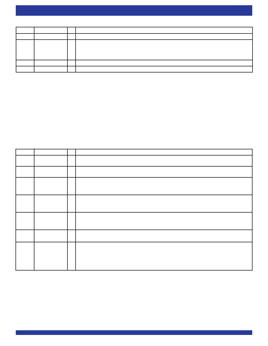
PIN DESCRIPTION (PBGA PACKAGE ONLY)
Symbol
Name
I/O
Description
ASYR(1)
Asynchronous
I
A HIGH on this input during Master Reset will select Synchronous read operation for the output port. A LOW
Read Port
will select Asynchronous operation. If Asynchronous is selected the FIFO must operate in IDT Standard mode.
ASYW(1)
Asynchronous
I
A HIGH on this input during Master Reset will select Synchronous write operation for the input port. A LOW
WritePort
will select Asynchronous operation.
TCK(2)
JTAG Clock
I
Clock input for JTAG function. One of four terminals required by IEEE Standard 1149.1-1990. Test operations of the
device are synchronous to TCK. Data from TMS and TDI are sampled on the rising edge of TCK and outputs change
on the falling edge of TCK. If the JTAG function is not used this signal needs to be tied to GND.
TDI(2)
JTAG Test Data
I
One of four terminals required by IEEE Standard 1149.1-1990. During the JTAG boundary scan operation, test data
Input
seriallyloadedviatheTDIontherisingedgeofTCKtoeithertheInstructionRegister,IDRegisterandBypassRegister.
An internal pull-up resistor forces TDI HIGH if left unconnected.
TDO(2)
JTAG Test Data
O
One of four terminals required by IEEE Standard 1149.1-1990. During the JTAG boundary scan operation, test data
Output
seriallyloadedoutputviatheTDOonthefallingedgeofTCKfromeithertheInstructionRegister,IDRegisterandBypass
Register. This output is high impedance except when shifting, while in SHIFT-DR and SHIFT-IR controller states.
TMS(2)
JTAG Mode Select
I
TMSisaserialinputpin.OneoffourterminalsrequiredbyIEEEStandard1149.1-1990.TMSdirectsthedevicethrough
its TAP controller states. An internal pull-up resistor forces TMS HIGH if left unconnected.
TRST(2)
JTAG Reset
I
TRST is an asynchronous reset pin for the JTAG controller. The JTAG TAP controller does not automatically reset
upon power-up, thus it must be reset by either this signal or by setting TMS= HIGH for five TCK cycles. If the TAP
controller is not properly reset then the FIFO outputs will always be in high-impedance. If the JTAG function is used
but the user does not want to use
TRST, then TRST can be tied with MRS to ensure proper FIFO operation. If the
JTAG function is not used then this signal needs to be tied to GND.
PIN DESCRIPTION-CONTINUED (TQFP & PBGA PACKAGES)
SEN
Serial Enable
I
SENenablesserialloadingofprogrammableflagoffsets.
WCLK/
WriteClock/
I
If Synchronous operation of the write port has been selected, when enabled by
WEN, the rising edge of WCLK
WR
WriteStrobe
writes data into the FIFO. If Asynchronous operation of the write port has been selected, WR writes data into the FIFO
on a rising edge in an Asynchronous manner, (
WEN should be tied to its active state). Asynchronous operation of
the WCLK/WR input is only available in the PBGA package.
WEN
WriteEnable
I
WEN enables WCLK for writing data into the FIFO memory and offset registers.
VCC
+3.3V Supply
I
These are VCC supply inputs and must be connected to the 3.3V supply rail.
Symbol
Name
I/O
Description
NOTE:
1. Inputs should not change state after Master Reset.
相关PDF资料 |
PDF描述 |
|---|---|
| MS27468T11B35S EDR | CONN RCPT 13POS JAM NUT W/SCKT |
| IDT72V3676L15PF8 | IC FIFO 16384X36 15NS 128QFP |
| MS3120P14-18S | CONN RCPT 18POS WALL MNT W/SCKT |
| IDT72V3674L15PF8 | IC FIFO 16384X36 15NS 128QFP |
| MS27467T11B35P EDR | CONN PLUG 13POS STRAIGHT W/PINS |
相关代理商/技术参数 |
参数描述 |
|---|---|
| IDT72V3680L10PFI | 制造商:Integrated Device Technology Inc 功能描述: |
| IDT72V3680L15PF | 功能描述:IC FIFO SS 16384X36 15NS 128TQFP RoHS:否 类别:集成电路 (IC) >> 逻辑 - FIFO 系列:72V 标准包装:15 系列:74F 功能:异步 存储容量:256(64 x 4) 数据速率:- 访问时间:- 电源电压:4.5 V ~ 5.5 V 工作温度:0°C ~ 70°C 安装类型:通孔 封装/外壳:24-DIP(0.300",7.62mm) 供应商设备封装:24-PDIP 包装:管件 其它名称:74F433 |
| IDT72V3680L15PF8 | 功能描述:IC FIFO SS 16384X36 15NS 128TQFP RoHS:否 类别:集成电路 (IC) >> 逻辑 - FIFO 系列:72V 标准包装:15 系列:74F 功能:异步 存储容量:256(64 x 4) 数据速率:- 访问时间:- 电源电压:4.5 V ~ 5.5 V 工作温度:0°C ~ 70°C 安装类型:通孔 封装/外壳:24-DIP(0.300",7.62mm) 供应商设备封装:24-PDIP 包装:管件 其它名称:74F433 |
| IDT72V3680L15PFI | 功能描述:IC FIFO SS 16384X36 15NS 128TQFP RoHS:否 类别:集成电路 (IC) >> 逻辑 - FIFO 系列:72V 标准包装:15 系列:74F 功能:异步 存储容量:256(64 x 4) 数据速率:- 访问时间:- 电源电压:4.5 V ~ 5.5 V 工作温度:0°C ~ 70°C 安装类型:通孔 封装/外壳:24-DIP(0.300",7.62mm) 供应商设备封装:24-PDIP 包装:管件 其它名称:74F433 |
| IDT72V3680L15PFI8 | 功能描述:IC FIFO SS 16384X36 15NS 128TQFP RoHS:否 类别:集成电路 (IC) >> 逻辑 - FIFO 系列:72V 标准包装:15 系列:74F 功能:异步 存储容量:256(64 x 4) 数据速率:- 访问时间:- 电源电压:4.5 V ~ 5.5 V 工作温度:0°C ~ 70°C 安装类型:通孔 封装/外壳:24-DIP(0.300",7.62mm) 供应商设备封装:24-PDIP 包装:管件 其它名称:74F433 |
发布紧急采购,3分钟左右您将得到回复。