- 您现在的位置:买卖IC网 > PDF目录9186 > IDT72V71623BC (IDT, Integrated Device Technology Inc)IC DGTL SW 2048X2048 144-BGA PDF资料下载
参数资料
| 型号: | IDT72V71623BC |
| 厂商: | IDT, Integrated Device Technology Inc |
| 文件页数: | 2/28页 |
| 文件大小: | 0K |
| 描述: | IC DGTL SW 2048X2048 144-BGA |
| 标准包装: | 14 |
| 系列: | 72V |
| 类型: | 多路复用器 |
| 电路: | 1 x 1:16 |
| 独立电路: | 1 |
| 电压电源: | 单电源 |
| 电源电压: | 3 V ~ 3.6 V |
| 工作温度: | -40°C ~ 85°C |
| 安装类型: | 表面贴装 |
| 封装/外壳: | 144-LBGA |
| 供应商设备封装: | 144-CABGA(13x13) |
| 包装: | 托盘 |
| 其它名称: | 72V71623BC |
第1页当前第2页第3页第4页第5页第6页第7页第8页第9页第10页第11页第12页第13页第14页第15页第16页第17页第18页第19页第20页第21页第22页第23页第24页第25页第26页第27页第28页
10
COMMERCIAL TEMPERATURE RANGE
IDT72V71623 3.3V TIME SLOT INTERCHANGE
DIGITAL SWITCH 2,048 x 2,048
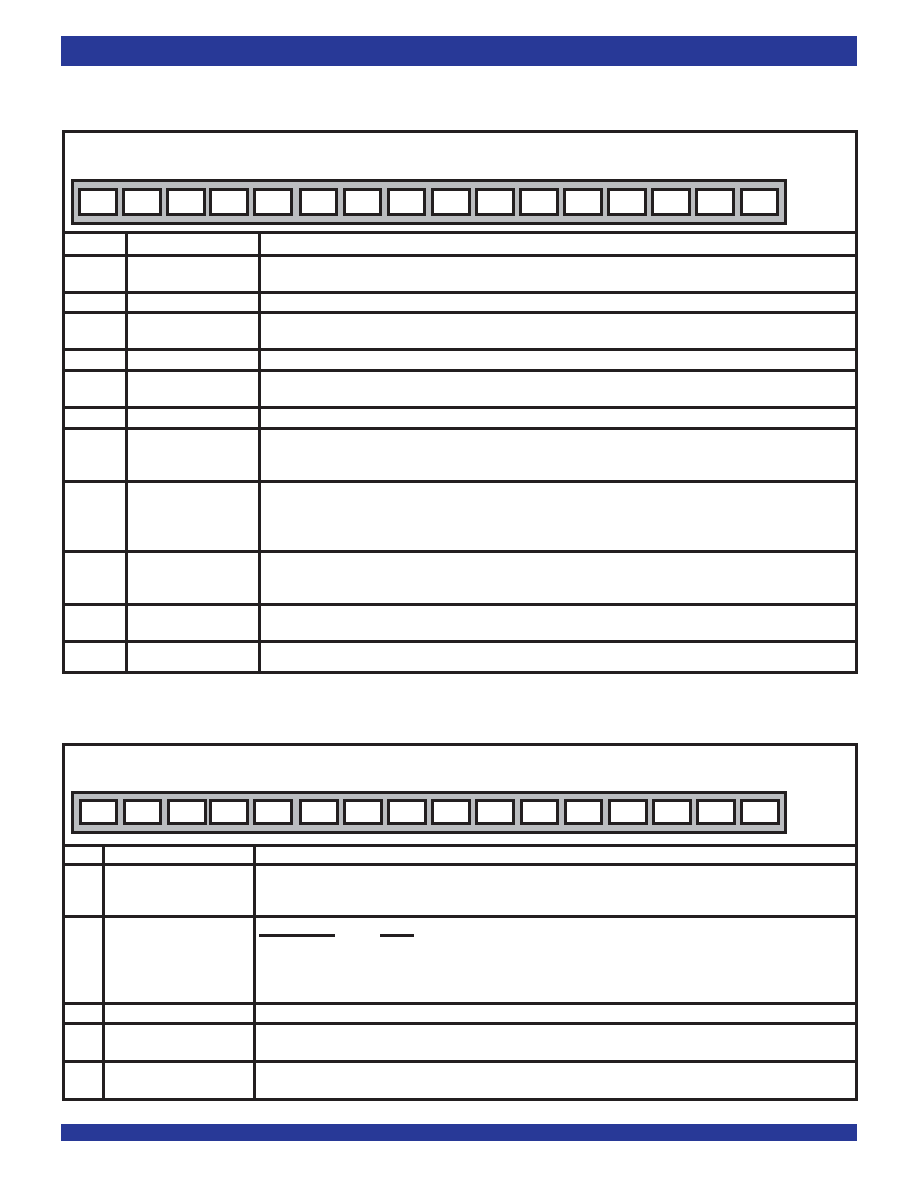
TABLE 3 — CONTROL REGISTER (CR) BITS
TABLE 4 — CONNECTION MEMORY BITS
ResetValue:
4000H.
Bit
Name
Description
15
Reset(SoftwareReset)
A one will reset the device and have the same effect as of the RESET pin. Must be zero for normal operation. Before beginning
operation,thisbitmustbeheldzeroforminimum100ns.
14
Unused
Mustbeoneforproperoperation.
13
OEPOL
When 1, a one on OEI pin denotes an active state on the output data stream; zero on OEI pin denotes high-impedance state.
(OutputEnablePolarity)
When0,aonedenoteshigh-impedanceandazerodenotesanactivestate.
12
Unused
Mustbezerofornormaloperation.
11
MBP
When1,theConnectionMemoryblockprogrammingfeatureisreadyfortheprogrammingofConnectionMemoryhighbits,
(Memory Block Program)
bit 13 to bit 15. When 0, this feature is disabled.
10
Unused
Mustbezerofornormaloperation.
9-7
BPD2-0
These bits carry the value to be loaded into the Connection Memory block whenever the memory block programming feature is
(BlockProgrammingData) activated. After the MBP bit in the control register is set to 1 and the BPE bit is set to 1, the contents of the bits BPD2-0 are
loaded into bit 15 and 13 of the Connection Memory. Bit 12 to bit 0 of the Connection Memory are set to 0.
6
BPE
Azerotoonetransitionofthisbitenablesthememoryblockprogrammingfunction.TheBPEandBPD2-0bitsintheCRregister
(BeginBlockProgramming have to be defined in the same write operation. Once the BPE bit is set HIGH, the device requires two frames to complete the
Enable)
blockprogramming.Aftertheprogrammingfunctionhasfinished,theBPEbitreturnstozerotoindicatetheoperationiscompleted.
WhentheBPE=1,theotherbitinthecontrolregistermustnotbechangedfortwoframestoensureproperoperation.
5
OSB
WhenODE=0andOSB=0,theoutputdriversoftransmitserialstreamsareinhigh-impedancemode.WhenODE=1orOSB=1,
(OutputStandBy)
ConnectionMemoryMod1-0
≠ 1and1,theoutputserialstreamdriversfunctionnormally.WhenbothConnectionMemoryMod
1 - 0 = 1 and 1, the output drivers of the transmit serial streams are in high impedance mode. Please refer to Table 1.
4
SFE
Azerotoonetransitioninthisbitstartstheframeevaluationprocedure.WhentheCFEbitintheFARregisterchangesfromzero
(StartFrameEvaluation)
toone,theevaluationprocedurestops.Tostartanotherframeevaluationcycle,setthisbittozeroforatleastoneframe.
3-0
DR3-0
Input/Outputdatarateselection.SeeTable5fordetailedprogramming.
15
14
13
12
11
10
9876543210
SRS
1
OEP
0
MBP
0
BPD2
BPD1
BPD0
BPE
OSB
SFE
DR3
DR2
DR1
DR0
Bit
Name
Description
15
LPBK
When 1, the RX n channel m data comes from the TX n channel m. For proper per channel loopback operations, set the delay
(PerChannelLoopback)
offset register bits OFn[2:0] to zero for the streams which are in the loopback mode. This feature is offered only when
DR3-0 = 0000, 0001 or 0010 is selected via the control register.
14,13 MOD1-0
MOD1 MOD0
MODE
(SwitchingModeSelection)
0
VariableDelaymode
0
1
ConstantDelaymode
1
0
Processormode
1
OutputHigh-Impedance
12
Unused
Mustbezerofornormaloperation.
11-8
SAB3-0
The binary value is the number of the data stream for the source of the connection. Unused SAB bits must be zero for proper
(Source Stream Address Bits) operation.
7-0
CAB7-0
The binary value is the number of the channel for the source of the connection. Unused CAB bits must be zero for proper
(Source Channel Address Bits) operation.
15
14
13
12
11
10
9876543210
LPBK MOD1 MOD0
0
SAB3
SAB2
SAB1
SAB0
CAB7
CAB6
CAB5
CAB4
CAB3
CAB2
CAB1
CAB0
相关PDF资料 |
PDF描述 |
|---|---|
| VI-BWX-MY-F3 | CONVERTER MOD DC/DC 5.2V 50W |
| VI-BWX-MY-F1 | CONVERTER MOD DC/DC 5.2V 50W |
| VI-BWW-MY-F4 | CONVERTER MOD DC/DC 5.5V 50W |
| MS3450W28-9PY | CONN RCPT 12POS WALL MNT W/PINS |
| IDT72V71623DAG | IC DGTL SW 2048X2048 144-TQFP |
相关代理商/技术参数 |
参数描述 |
|---|---|
| IDT72V71623BC8 | 功能描述:IC DGTL SW 2048X2048 144-BGA RoHS:否 类别:集成电路 (IC) >> 逻辑 - 信号开关,多路复用器,解码器 系列:72V 标准包装:48 系列:74VHC 类型:多路复用器 电路:4 x 2:1 独立电路:1 输出电流高,低:8mA,8mA 电压电源:单电源 电源电压:2 V ~ 5.5 V 工作温度:-40°C ~ 85°C 安装类型:表面贴装 封装/外壳:16-SOIC(0.154",3.90mm 宽) 供应商设备封装:16-SOIC 包装:管件 |
| IDT72V71623BCG | 功能描述:IC DGTL SW 2048X2048 144-BGA RoHS:是 类别:集成电路 (IC) >> 逻辑 - 信号开关,多路复用器,解码器 系列:72V 标准包装:48 系列:74VHC 类型:多路复用器 电路:4 x 2:1 独立电路:1 输出电流高,低:8mA,8mA 电压电源:单电源 电源电压:2 V ~ 5.5 V 工作温度:-40°C ~ 85°C 安装类型:表面贴装 封装/外壳:16-SOIC(0.154",3.90mm 宽) 供应商设备封装:16-SOIC 包装:管件 |
| IDT72V71623BCG8 | 功能描述:IC DGTL SW 2048X2048 144-BGA RoHS:是 类别:集成电路 (IC) >> 逻辑 - 信号开关,多路复用器,解码器 系列:72V 标准包装:48 系列:74VHC 类型:多路复用器 电路:4 x 2:1 独立电路:1 输出电流高,低:8mA,8mA 电压电源:单电源 电源电压:2 V ~ 5.5 V 工作温度:-40°C ~ 85°C 安装类型:表面贴装 封装/外壳:16-SOIC(0.154",3.90mm 宽) 供应商设备封装:16-SOIC 包装:管件 |
| IDT72V71623DA | 功能描述:IC DGTL SW 2048X2048 144-TQFP RoHS:否 类别:集成电路 (IC) >> 逻辑 - 信号开关,多路复用器,解码器 系列:72V 标准包装:48 系列:74VHC 类型:多路复用器 电路:4 x 2:1 独立电路:1 输出电流高,低:8mA,8mA 电压电源:单电源 电源电压:2 V ~ 5.5 V 工作温度:-40°C ~ 85°C 安装类型:表面贴装 封装/外壳:16-SOIC(0.154",3.90mm 宽) 供应商设备封装:16-SOIC 包装:管件 |
| IDT72V71623DAG | 功能描述:IC DGTL SW 2048X2048 144-TQFP RoHS:是 类别:集成电路 (IC) >> 逻辑 - 信号开关,多路复用器,解码器 系列:72V 标准包装:48 系列:74VHC 类型:多路复用器 电路:4 x 2:1 独立电路:1 输出电流高,低:8mA,8mA 电压电源:单电源 电源电压:2 V ~ 5.5 V 工作温度:-40°C ~ 85°C 安装类型:表面贴装 封装/外壳:16-SOIC(0.154",3.90mm 宽) 供应商设备封装:16-SOIC 包装:管件 |
发布紧急采购,3分钟左右您将得到回复。