- 您现在的位置:买卖IC网 > PDF目录4579 > IDT77V500S25BC (IDT, Integrated Device Technology Inc)IC SW MEMORY 8X8 1.2BGPS 144-BGA PDF资料下载
参数资料
| 型号: | IDT77V500S25BC |
| 厂商: | IDT, Integrated Device Technology Inc |
| 文件页数: | 3/17页 |
| 文件大小: | 0K |
| 描述: | IC SW MEMORY 8X8 1.2BGPS 144-BGA |
| 标准包装: | 126 |
| 系列: | SwitchStar™ |
| 类型: | 集成式开关控制器 |
| 安装类型: | 表面贴装 |
| 封装/外壳: | 144-LBGA |
| 供应商设备封装: | 144-CABGA(13x13) |
| 包装: | 托盘 |
| 其它名称: | 77V500S25BC |
11 of 17
April 11, 2001
IDT77V500
CBR Clock Parameters
"x" for this waveform represents either 2 or 3, depending on which CBRCLK is used (CBRCLK2 or CBRCLK3).
CBRCLKx
tCLx
tCHx
tCYCx
3607 drw 11
the pointer should be moved back to the top of the CBR VC List if all the
VCs in the list have been serviced. Thus the user can establish a frame
duration and be assured that a cell from each VC in the OPyCBRx VC
List is transmitted in each frame time. Sub lists can also be established
within the CBR VC List so that a particular VC could be weighted to ship
more cells per frame than the others.
Example 2 illustrates using very slow CBR clocks (tCHx greater than
or equal to 8 SCLKs) to shape traffic in a VBR form of implementation. A
cell from a VC on the OPyCBRx VC List is again scheduled on each
rising clock edge of SCLK after a falling edge of CBRCLKx, but since
tCHx is HIGH for more than eight SCLKs, there is more direct control
over the exact time in which each cell of the VC List is scheduled. The
single cell will then be transmitted when the output is available and other
previously scheduled Input and Output ports of the IDT77V400 have
been serviced (there is again the potential delay based on other traffic
passing through the IDT77V400). The IDT77V500 will service all of the
VCs in the OPyCBRx VC List because the count will prevent the pointer
from returning to the top of the CBR VC List until all VCs on the list with
cells have been serviced. The user can thus more closely manage the
transmission of cells with this slower CBR clock rate because it is more
directly related to individual CBRCLKx High-to-Low transitions.
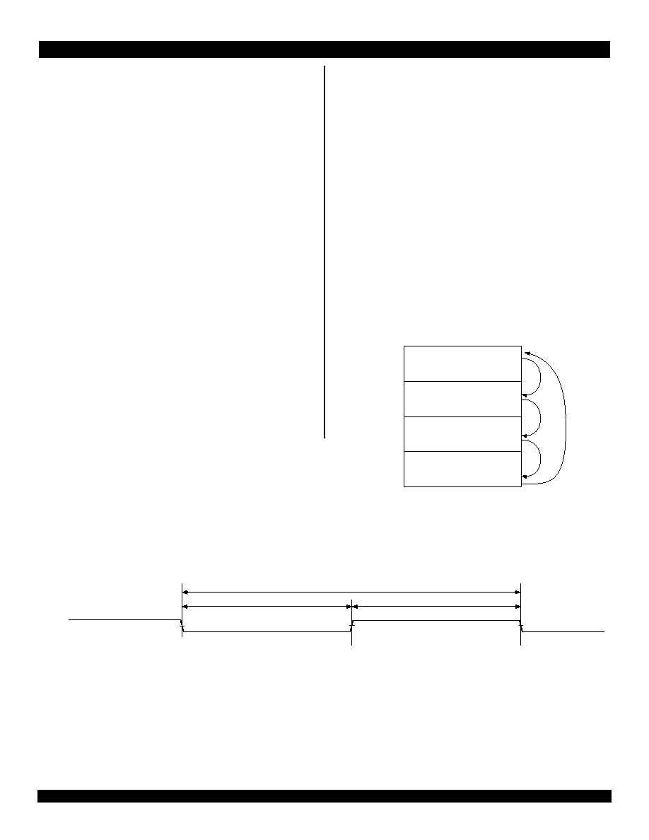
Figure 3 OPyBRx VC Example
3607 drw 10
100
200
300
400
Beginning
End
CBR Functional Description
The Constant Bit Rate (CBR) functionality of the IDT77V500 provides
both the opportunity for scheduling priority traffic at a regular interval and
traffic shaping capability. Two external CBR clocks, CBRCLK3 and
CBRCLK2, are available and associated with Output Priority 3 (Highest
Priority) and Priority 2 respectively. Calls assigned to a particular CBR
VC in the IDT77V500 Per VC Table are linked together in a CBR Per VC
list by output, so that a cell from each VC of a particular CBR Per VC list
are serviced on each cycle through the list. The CBR Per VC List is iden-
tified by both the output and CBR priority on that output; for example,
OPyCBRx VC list represents Output y (Output number 0-7) and CBR
priority x (CBR priority 3 or 2). Figure 3 is an example of an OPyCBRx
VC List with four VCs in the list: 100 (the first entry in the list), 200, 300
and 400. The arrows indicate the linking sequence in this VC List. Figure
3 will be used with the CBR Clock Functional Waveforms to illustrate two
basic functional implementations using the CBR Clocks.
CBR Clock Functional Waveform Example 1 uses the CBR clocks to
frame execution of the OPyCBRx VC List. A cell from a specific VC on
the OPyCBRx VC List is scheduled on each rising clock edge of SCLK
after a falling edge of CBRCLKx. The cell will then be transmitted when
output y is available and other previously scheduled Input and Output
ports of the IDT77V400 have been serviced. This delay can be as long
as 65 SCLK cycles maximum for each cell in the Service Class 3 CBR
VC List, although it will typically be significantly less. The Service Class
2 delay can be larger if there is higher priority traffic to be transmitted.
This delay needs to be taken into account, as the next cell in the
OPyCBRx VC List will not be scheduled until the previous cell in the list
has been serviced. Thus enough CBRCLKx pulses need to be provided
to make sure all potential cells in the OPyCBRx VC List are scheduled.
This waveform illustrates the ideal case of each cell being immediately
transmitted after scheduling, enabling the scheduling and transmission
of the next cell in the OPyCBRxVC List on the next SCLK rising edge.
CBRCLKx HIGH for eight SCLK cycles or more tells the controller that
相关PDF资料 |
PDF描述 |
|---|---|
| IDT77V500S25BCG | IC SW MEMORY 8X8 1.2BGPS 144-BGA |
| EB81-S0K2240X | CONN EDGEBOARD DUAL 44POS 5A |
| LT1175IS8-5#TRPBF | IC REG LDO -5V .5A 8SOIC |
| RMM43DTMD | CONN EDGECARD 86POS R/A .156 SLD |
| LFXP10C-4F256I | IC FPGA 9.7KLUTS 188I/O 256-BGA |
相关代理商/技术参数 |
参数描述 |
|---|---|
| IDT77V500S25BC8 | 功能描述:IC SW MEMORY 8X8 1.2BGPS 144-BGA RoHS:否 类别:集成电路 (IC) >> 专用 IC 系列:SwitchStar™ 产品培训模块:Lead (SnPb) Finish for COTS Obsolescence Mitigation Program 标准包装:1 系列:- 类型:调帧器 应用:数据传输 安装类型:表面贴装 封装/外壳:400-BBGA 供应商设备封装:400-PBGA(27x27) 包装:散装 |
| IDT77V500S25BCG | 功能描述:IC SW MEMORY 8X8 1.2BGPS 144-BGA RoHS:是 类别:集成电路 (IC) >> 专用 IC 系列:SwitchStar™ 产品培训模块:Lead (SnPb) Finish for COTS Obsolescence Mitigation Program 标准包装:1 系列:- 类型:调帧器 应用:数据传输 安装类型:表面贴装 封装/外壳:400-BBGA 供应商设备封装:400-PBGA(27x27) 包装:散装 |
| IDT77V500S25BCG8 | 功能描述:IC SW MEMORY 8X8 1.2BGPS 144-BGA RoHS:是 类别:集成电路 (IC) >> 专用 IC 系列:SwitchStar™ 产品培训模块:Lead (SnPb) Finish for COTS Obsolescence Mitigation Program 标准包装:1 系列:- 类型:调帧器 应用:数据传输 安装类型:表面贴装 封装/外壳:400-BBGA 供应商设备封装:400-PBGA(27x27) 包装:散装 |
| IDT77V500S25PF | 功能描述:IC SW MEMORY 8X8 1.2BGPS 100TQFP RoHS:否 类别:集成电路 (IC) >> 专用 IC 系列:SwitchStar™ 产品培训模块:Lead (SnPb) Finish for COTS Obsolescence Mitigation Program 标准包装:1 系列:- 类型:调帧器 应用:数据传输 安装类型:表面贴装 封装/外壳:400-BBGA 供应商设备封装:400-PBGA(27x27) 包装:散装 |
| IDT77V500S25PF8 | 功能描述:IC SW MEMORY 8X8 1.2BGPS 100TQFP RoHS:否 类别:集成电路 (IC) >> 专用 IC 系列:SwitchStar™ 产品培训模块:Lead (SnPb) Finish for COTS Obsolescence Mitigation Program 标准包装:1 系列:- 类型:调帧器 应用:数据传输 安装类型:表面贴装 封装/外壳:400-BBGA 供应商设备封装:400-PBGA(27x27) 包装:散装 |
发布紧急采购,3分钟左右您将得到回复。