- 您现在的位置:买卖IC网 > PDF目录4579 > IDT77V500S25BC (IDT, Integrated Device Technology Inc)IC SW MEMORY 8X8 1.2BGPS 144-BGA PDF资料下载
参数资料
| 型号: | IDT77V500S25BC |
| 厂商: | IDT, Integrated Device Technology Inc |
| 文件页数: | 4/17页 |
| 文件大小: | 0K |
| 描述: | IC SW MEMORY 8X8 1.2BGPS 144-BGA |
| 标准包装: | 126 |
| 系列: | SwitchStar™ |
| 类型: | 集成式开关控制器 |
| 安装类型: | 表面贴装 |
| 封装/外壳: | 144-LBGA |
| 供应商设备封装: | 144-CABGA(13x13) |
| 包装: | 托盘 |
| 其它名称: | 77V500S25BC |
12 of 17
April 11, 2001
IDT77V500
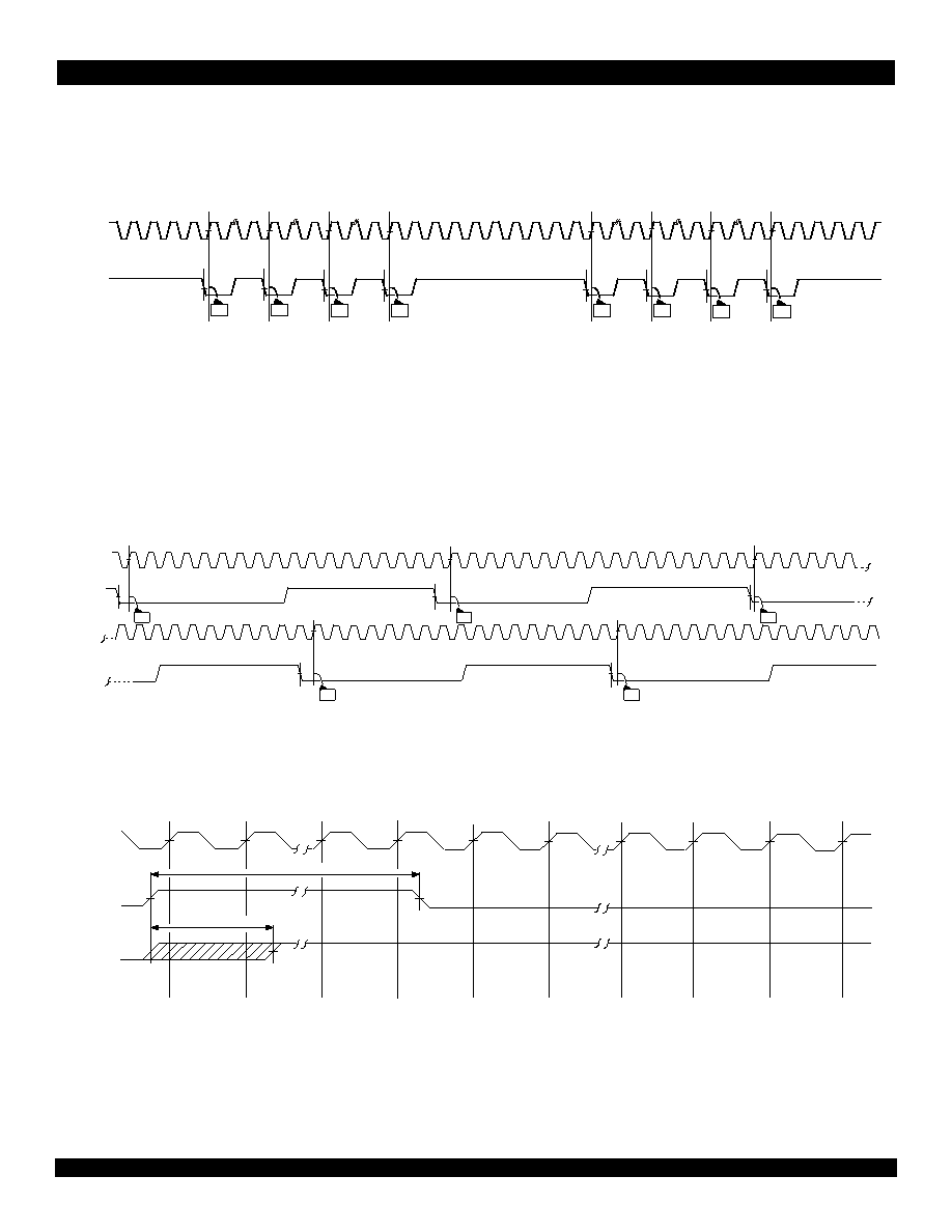
CBR Clock Functional Waveform Example 1 - CBR Frame Implementation
(Fast CBRCLK with Frame Timing)
This example shows the procedure recommended for use of direct CBR scheduling. "x" for this waveform represents either 2 or 3, depending on
which CBRCLK is used (CBRCLK2 or CBRCLK3) ("y" represents the specific output (0-7)). The OPyCBRx VC List for this example is defined in Figure
1A cell from a VC on the OPyCBRx VC List is scheduled on each rising clock edge of SCLK after a falling edge of CBRCLKx if the previous VC has completed internal processing.
2This example shows four VCs in the OPyCBRx VC List. The number of VCs in the OPxCBRx VC List may be as large as 8192.
3The period between reinitiation of the OPyCBRx VC List defines the frame size; that is, the amount of time between starting the transmissions from the top of the OPyCBRx VC List.
CBRCLKx must be HIGH for eight clocks or more to reinitiate the transmission sequence at the start of the OPyCBRx VC List.
CBR Clock Functional Waveform Example 2 - VBR/CBR Implementation
(t
(tCH
CH
x > 8 SCLK)
This example shows the use of a slower CBRCLK (tCHx > 8 SCLK) to provide VBR/CBR traffic shaping. For this waveform "x" represents either 2
or 3, depending on which CBRCLK is used (CBRCLK2 or CBRCLK3). ("y" represents the specific output (0-7)) The OPyCBRx VC List for this example
is defined in Figure 3.
1A cell from a VC on the OPyCBRx VC List is scheduled on each rising edge of SCLK after a falling edge of CBRCLKx.
2tCHx > 8 SCLK so that a cell is scheduled after each falling edge of CBRCLKx.
3The pointer has moved back to the beginning of the OPyCBRx VC List.
Reset Waveforms
1RESETI must be held HIGH for 8 SCLK cycles. When RESETI goes Low again 8191 cycles are used prior to the Status Acknowledge bits showing the internal reset process is com-
plete.
2This delay should typically be much less than two SCLK cycles. RESETO remains High until START Command is received from the Call Setup Manager.
12
SCLK
CBRCLKx
100
200
300
400
3
100
200
300
400
12
3607 drw 12
100
SCLK
2
cont'd
waveform
CBRCLKx
1
see cont'd
waveform
3607 drw 13
3
200
300
100
400
SCLK
RESETI
3607 drw 14
1
2
781
2
8190
8191
1
tRSI
RESETO
1
2
2 clock cycles max.
相关PDF资料 |
PDF描述 |
|---|---|
| IDT77V500S25BCG | IC SW MEMORY 8X8 1.2BGPS 144-BGA |
| EB81-S0K2240X | CONN EDGEBOARD DUAL 44POS 5A |
| LT1175IS8-5#TRPBF | IC REG LDO -5V .5A 8SOIC |
| RMM43DTMD | CONN EDGECARD 86POS R/A .156 SLD |
| LFXP10C-4F256I | IC FPGA 9.7KLUTS 188I/O 256-BGA |
相关代理商/技术参数 |
参数描述 |
|---|---|
| IDT77V500S25BC8 | 功能描述:IC SW MEMORY 8X8 1.2BGPS 144-BGA RoHS:否 类别:集成电路 (IC) >> 专用 IC 系列:SwitchStar™ 产品培训模块:Lead (SnPb) Finish for COTS Obsolescence Mitigation Program 标准包装:1 系列:- 类型:调帧器 应用:数据传输 安装类型:表面贴装 封装/外壳:400-BBGA 供应商设备封装:400-PBGA(27x27) 包装:散装 |
| IDT77V500S25BCG | 功能描述:IC SW MEMORY 8X8 1.2BGPS 144-BGA RoHS:是 类别:集成电路 (IC) >> 专用 IC 系列:SwitchStar™ 产品培训模块:Lead (SnPb) Finish for COTS Obsolescence Mitigation Program 标准包装:1 系列:- 类型:调帧器 应用:数据传输 安装类型:表面贴装 封装/外壳:400-BBGA 供应商设备封装:400-PBGA(27x27) 包装:散装 |
| IDT77V500S25BCG8 | 功能描述:IC SW MEMORY 8X8 1.2BGPS 144-BGA RoHS:是 类别:集成电路 (IC) >> 专用 IC 系列:SwitchStar™ 产品培训模块:Lead (SnPb) Finish for COTS Obsolescence Mitigation Program 标准包装:1 系列:- 类型:调帧器 应用:数据传输 安装类型:表面贴装 封装/外壳:400-BBGA 供应商设备封装:400-PBGA(27x27) 包装:散装 |
| IDT77V500S25PF | 功能描述:IC SW MEMORY 8X8 1.2BGPS 100TQFP RoHS:否 类别:集成电路 (IC) >> 专用 IC 系列:SwitchStar™ 产品培训模块:Lead (SnPb) Finish for COTS Obsolescence Mitigation Program 标准包装:1 系列:- 类型:调帧器 应用:数据传输 安装类型:表面贴装 封装/外壳:400-BBGA 供应商设备封装:400-PBGA(27x27) 包装:散装 |
| IDT77V500S25PF8 | 功能描述:IC SW MEMORY 8X8 1.2BGPS 100TQFP RoHS:否 类别:集成电路 (IC) >> 专用 IC 系列:SwitchStar™ 产品培训模块:Lead (SnPb) Finish for COTS Obsolescence Mitigation Program 标准包装:1 系列:- 类型:调帧器 应用:数据传输 安装类型:表面贴装 封装/外壳:400-BBGA 供应商设备封装:400-PBGA(27x27) 包装:散装 |
发布紧急采购,3分钟左右您将得到回复。