- 您现在的位置:买卖IC网 > PDF目录9973 > IDT82V2041EPP8 (IDT, Integrated Device Technology Inc)IC LIU T1/J1/E1 1CH 44-TQFP PDF资料下载
参数资料
| 型号: | IDT82V2041EPP8 |
| 厂商: | IDT, Integrated Device Technology Inc |
| 文件页数: | 17/75页 |
| 文件大小: | 0K |
| 描述: | IC LIU T1/J1/E1 1CH 44-TQFP |
| 标准包装: | 1,250 |
| 类型: | 线路接口装置(LIU) |
| 规程: | E1 |
| 电源电压: | 3.13 V ~ 3.47 V |
| 安装类型: | 表面贴装 |
| 封装/外壳: | 44-LQFP |
| 供应商设备封装: | 44-TQFP(10x10) |
| 包装: | 带卷 (TR) |
| 其它名称: | 82V2041EPP8 |
第1页第2页第3页第4页第5页第6页第7页第8页第9页第10页第11页第12页第13页第14页第15页第16页当前第17页第18页第19页第20页第21页第22页第23页第24页第25页第26页第27页第28页第29页第30页第31页第32页第33页第34页第35页第36页第37页第38页第39页第40页第41页第42页第43页第44页第45页第46页第47页第48页第49页第50页第51页第52页第53页第54页第55页第56页第57页第58页第59页第60页第61页第62页第63页第64页第65页第66页第67页第68页第69页第70页第71页第72页第73页第74页第75页
IDT82V2041E
SINGLE CHANNEL T1/E1/J1 SHORT HAUL LINE INTERFACE UNIT
Functional Description
24
December 9, 2005
3.4.8
RECEIVE PATH SYSTEM INTERFACE
The receive path system interface consists of RCLK pin, RD/RDP pin
and RDN pin. In E1 mode, the RCLK outputs a recovered 2.048 MHz clock.
In T1/J1 mode, the RCLK outputs a recovered 1.544 MHz clock. The
received data is updated on the RD/RDP and RDN pins on the active edge
of RCLK. The active edge of RCLK can be selected by the RCLK_SEL bit
(RCF0, 0AH). And the active level of the data on RD/RDP and RDN can be
selected by the RD_INV bit (RCF0, 0AH).
In hardware control mode, only the active edge of RCLK can be
selected.IfRCLKEissettohigh,thefallingedgewillbechosenastheactive
edge of RCLK. If RCLKE is set to low, the rising edge will be chosen as the
active edge of RCLK. The active level of the data on RD/RDP and RDN is
the same as that in software control mode.
Thereceiveddatacanbeoutputtothesystemsideintwodifferentways:
Single Rail or Dual Rail, as selected by R_MD bit [1] (RCF0, 0AH). In Single
Rail mode, only RD pin is used to output data and the RDN/CV pin is used
to report the received errors. In Dual Rail Mode, both RDP pin and RDN pin
are used for outputting data.
In the receive Dual Rail mode, the CDR unit can be by-passed by setting
R_MD[1:0] to ‘11’ (binary). In this situation, the output data from the Data
Slicer will be output to the RDP/RDN pins directly, and the RCLK outputs
the exclusive OR (XOR) of the RDP and RDN. This is called receiver slicer
mode. In this case, the transmit path is still operating in Dual Rail mode.
3.4.9
RECEIVE PATH POWER DOWN
The receive path can be powered down by setting R_OFF bit (RCF0,
0AH) to‘1’.Inthiscase, the RCLK,RD/RDP,RDNandLOSwillbelogiclow.
In hardware control mode, receiverpower down can be selected by pull-
ing RPD pin to high. Refer to 5 Hardware Control Pin Summary for more
details.
3.5
JITTER ATTENUATOR
There is one JitterAttenuator in the IDT82V2041E.TheJitter Attenuator
can be deployed in the transmit path or the receive path, and can also be
disabled. This is selected by the JACF[1:0] bits (JACF, 04H).
In hardware control mode, Jitter Attenuator position, bandwidth and the
depth of FIFO can be selected by JA[1:0] pins. Refer to 5 Hardware Control
Pin Summary for details.
3.5.1
JITTER ATTENUATION FUNCTION DESCRIPTON
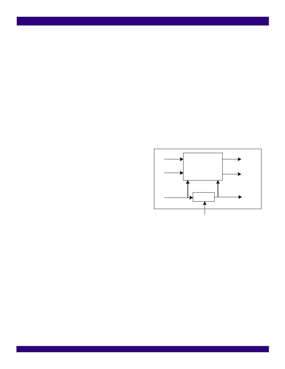
The Jitter Attenuator is composed of a FIFO and a DPLL, as shown in
Figure-11. The FIFO is used as a pool to buffer the jittered input data, then
the data is clocked out of the FIFO by a de-jittered clock. The depth of the
FIFO can be 32 bits, 64 bits or 128 bits, as selected by the JADP[1:0] bits
(JACF, 04H). In hardware control mode, the depth of FIFO can be selected
by JA[1:0] pins. Refer to 5 Hardware Control Pin Summary for details. Con-
sequently, the constant delay of the Jitter Attenuator will be 16 bits, 32 bits
or 64 bits. Deeper FIFO can tolerate larger jitter, butat the cost of increasing
data latency time.
Figure-11 Jitter Attenuator
In E1 applications, the Corner Frequency of the DPLL can be 0.9 Hz or
6.8 Hz, as selected by the JABW bit (JACF, 04H). In T1/J1 applications,
the Corner Frequency of the DPLL can be 1.25 Hz or 5.00 Hz, as selected
bytheJABWbit(JACF,04H).ThelowertheCornerFrequencyis,thelonger
time is needed to achieve synchronization.
When the incoming data moves faster than the outgoing data, the FIFO
will overflow. This overflow is captured by the JAOV_IS bit (INTS1, 1AH).
If the incoming data moves slower than the outgoing data, the FIFO will
underflow. This underflow is captured by the JAUD_IS bit (INTS1, 1AH). For
some applications that are sensitive to data corruption, the JA limit mode
can be enabled by setting JA_LIMIT bit (JACF, 04H) to ‘1’. In the JA limit
mode, the speed of the outgoing data will be adjusted automatically when
theFIFOisclosetoitsfulloremptiness.Thecriteriaofstartingspeedadjust-
ment are shown in Table-12. The JA limit mode can reduce the possibility
of FIFO overflow and underflow, but the quality of jitter attenuation is dete-
riorated.
FIFO
32/64/128
DPLL
Jittered Data
De-jittered Data
Jittered Clock
De-jittered Clock
MCLK
W
R
RCLK
RD/RDP
RDN
相关PDF资料 |
PDF描述 |
|---|---|
| VE-B5B-IV-F1 | CONVERTER MOD DC/DC 95V 150W |
| VE-26W-IX-B1 | CONVERTER MOD DC/DC 5.5V 75W |
| MS3100E28-10S | CONN RCPT 7POS WALL MNT W/SCKT |
| IDT72605L25PF | IC FIFO BI SYNC 256X18 64-TQFP |
| MS3100E22-20P | CONN RCPT 9POS WALL MNT W/PINS |
相关代理商/技术参数 |
参数描述 |
|---|---|
| IDT82V2041EPPG | 功能描述:IC LIU T1/J1/E1 1CH 44-TQFP RoHS:是 类别:集成电路 (IC) >> 接口 - 驱动器,接收器,收发器 系列:- 标准包装:250 系列:- 类型:收发器 驱动器/接收器数:2/2 规程:RS232 电源电压:3 V ~ 5.5 V 安装类型:表面贴装 封装/外壳:16-TSSOP(0.173",4.40mm 宽) 供应商设备封装:16-TSSOP 包装:带卷 (TR) |
| IDT82V2041EPPG8 | 功能描述:IC LIU T1/J1/E1 1CH 44-TQFP RoHS:是 类别:集成电路 (IC) >> 接口 - 驱动器,接收器,收发器 系列:- 标准包装:250 系列:- 类型:收发器 驱动器/接收器数:2/2 规程:RS232 电源电压:3 V ~ 5.5 V 安装类型:表面贴装 封装/外壳:16-TSSOP(0.173",4.40mm 宽) 供应商设备封装:16-TSSOP 包装:带卷 (TR) |
| IDT82V2042EPF | 功能描述:IC LIU T1/J1/E1 2CH SHORT 80TQFP RoHS:否 类别:集成电路 (IC) >> 接口 - 驱动器,接收器,收发器 系列:- 标准包装:250 系列:- 类型:收发器 驱动器/接收器数:2/2 规程:RS232 电源电压:3 V ~ 5.5 V 安装类型:表面贴装 封装/外壳:16-TSSOP(0.173",4.40mm 宽) 供应商设备封装:16-TSSOP 包装:带卷 (TR) |
| IDT82V2042EPF8 | 功能描述:IC LIU T1/J1/E1 2CH SHORT 80TQFP RoHS:否 类别:集成电路 (IC) >> 接口 - 驱动器,接收器,收发器 系列:- 标准包装:250 系列:- 类型:收发器 驱动器/接收器数:2/2 规程:RS232 电源电压:3 V ~ 5.5 V 安装类型:表面贴装 封装/外壳:16-TSSOP(0.173",4.40mm 宽) 供应商设备封装:16-TSSOP 包装:带卷 (TR) |
| IDT82V2042EPFG | 功能描述:IC LIU T1/J1/E1 2CH SHORT 80TQFP RoHS:是 类别:集成电路 (IC) >> 接口 - 驱动器,接收器,收发器 系列:- 标准包装:250 系列:- 类型:收发器 驱动器/接收器数:2/2 规程:RS232 电源电压:3 V ~ 5.5 V 安装类型:表面贴装 封装/外壳:16-TSSOP(0.173",4.40mm 宽) 供应商设备封装:16-TSSOP 包装:带卷 (TR) |
发布紧急采购,3分钟左右您将得到回复。