- 您现在的位置:买卖IC网 > PDF目录9970 > IDT82V2048BBG (IDT, Integrated Device Technology Inc)IC LIU T1/E1 8CH SHORT 160-BGA PDF资料下载
参数资料
| 型号: | IDT82V2048BBG |
| 厂商: | IDT, Integrated Device Technology Inc |
| 文件页数: | 6/62页 |
| 文件大小: | 0K |
| 描述: | IC LIU T1/E1 8CH SHORT 160-BGA |
| 标准包装: | 14 |
| 类型: | 线路接口装置(LIU) |
| 规程: | E1 |
| 电源电压: | 3.13 V ~ 3.47 V |
| 安装类型: | 表面贴装 |
| 封装/外壳: | 160-BGA |
| 供应商设备封装: | 160-PBGA(15x15) |
| 包装: | 托盘 |
| 其它名称: | 82V2048BBG |
第1页第2页第3页第4页第5页当前第6页第7页第8页第9页第10页第11页第12页第13页第14页第15页第16页第17页第18页第19页第20页第21页第22页第23页第24页第25页第26页第27页第28页第29页第30页第31页第32页第33页第34页第35页第36页第37页第38页第39页第40页第41页第42页第43页第44页第45页第46页第47页第48页第49页第50页第51页第52页第53页第54页第55页第56页第57页第58页第59页第60页第61页第62页
14
IDT82V2048 OCTAL T1/E1 SHORT HAUL LINE INTERFACE UNIT
INDUSTRIAL TEMPERATURE RANGES
2.3
CLOCK EDGES
The active edge of RCLKn and SCLK are selectable. If pin CLKE is
high, the active edge of RCLKn is the rising edge, as for SCLK, that is
falling edge. On the contrary, if CLKE is low, the active edge of RCLK is
the falling edge and that of SCLK is rising edge. Pins RDn/RDPn, CVn/
RDNn and SDO are always active high, and those output signals are
clocked out on the active edge of RCLKn and SCLK respectively. See
However, in dual rail mode without clock recovery, pin CLKE is used to
set the active level for RDPn/RDNn raw slicing output: High for active
high polarity and low for active low. It should be noted that data on pin
SDI are always active high and are sampled on the rising edges of
SCLK. The data on pin TDn/TDPn or BPVIn/TDNn are also always
active high but are sampled on the falling edges of TCLKn, despite the
level on CLKE.
2.4
RECEIVER
In receive path, the line signals couple into RRINGn and RTIPn via a
transformer and are converted into RZ digital pulses by a data slicer.
Adaptation for attenuation is achieved using an integral peak detector
that sets the slicing levels. Clock and data are recovered from the
received RZ digital pulses by a digital phase-locked loop that provides
jitter accommodation. After passing through the selectable jitter attenu-
ator, the recovered data are decoded using B8ZS/HDB3 or AMI line
code rules and clocked out of pin RDn in single rail mode, or presented
on RDPn/RDNn in an undecoded dual rail NRZ format. Loss of signal,
alarm indication signal, line code violation and excessive zeros are
detected. The presence of programmable inband loopback codes are
also detected. These various changes in status may be enabled to
generate interrupts.
2.4.1
PEAK DETECTOR AND SLICER
The slicer determines the presence and polarity of the received
pulses. In data recovery mode, the raw positive slicer output appears on
RDPn while the negative slicer output appears on RDNn. In clock and
data recovery mode, the slicer output is sent to Clock and Data
Recovery circuit for abstracting retimed data and optional decoding. The
slicer circuit has a built-in peak detector from which the slicing threshold
is derived. The slicing threshold is default to 50% (typical) of the peak
value.
Signals with an attenuation of up to 12 dB (from 2.4 V) can be recov-
ered by the receiver. To provide immunity from impulsive noise, the peak
detectors are held above a minimum level of 0.150 V typically, despite
the received signal level.
2.4.2
CLOCK AND DATA RECOVERY
The Clock and Data Recovery is accomplished by Digital Phase
Locked Loop (DPLL). The DPLL is clocked 16 times of the received
clock rate, i.e. 24.704 MHz in T1 mode or 32.768 MHz in E1 mode. The
recovered data and clock from DPLL is then sent to the selectable Jitter
Attenuator or decoder for further processing.
The clock recovery and data recovery mode can be selected on a per
channel basis by setting bit CRSn in register e-CRS. When bit CRSn is
defaulted to ‘0’, the corresponding channel operates in data and clock
recovery mode. The recovered clock is output on pin RCLKn and re-
timed NRZ data are output on pin RDPn/RDNn in dual rail mode or on
RDn in single rail mode. When bit CRSn is set to ‘1’, dual rail mode with
data recovery is enabled in the corresponding channel and the clock
recovery is bypassed. In this condition, the analog line signals are
converted to RZ digital bit streams on the RDPn/RDNn pins and inter-
nally connected to an EXOR which is fed to the RCLKn output for
external clock recovery applications.
If MCLK is pulled high, all the receivers will enter the dual rail mode
with data recovery. In this case, register e-CRS is ignored.
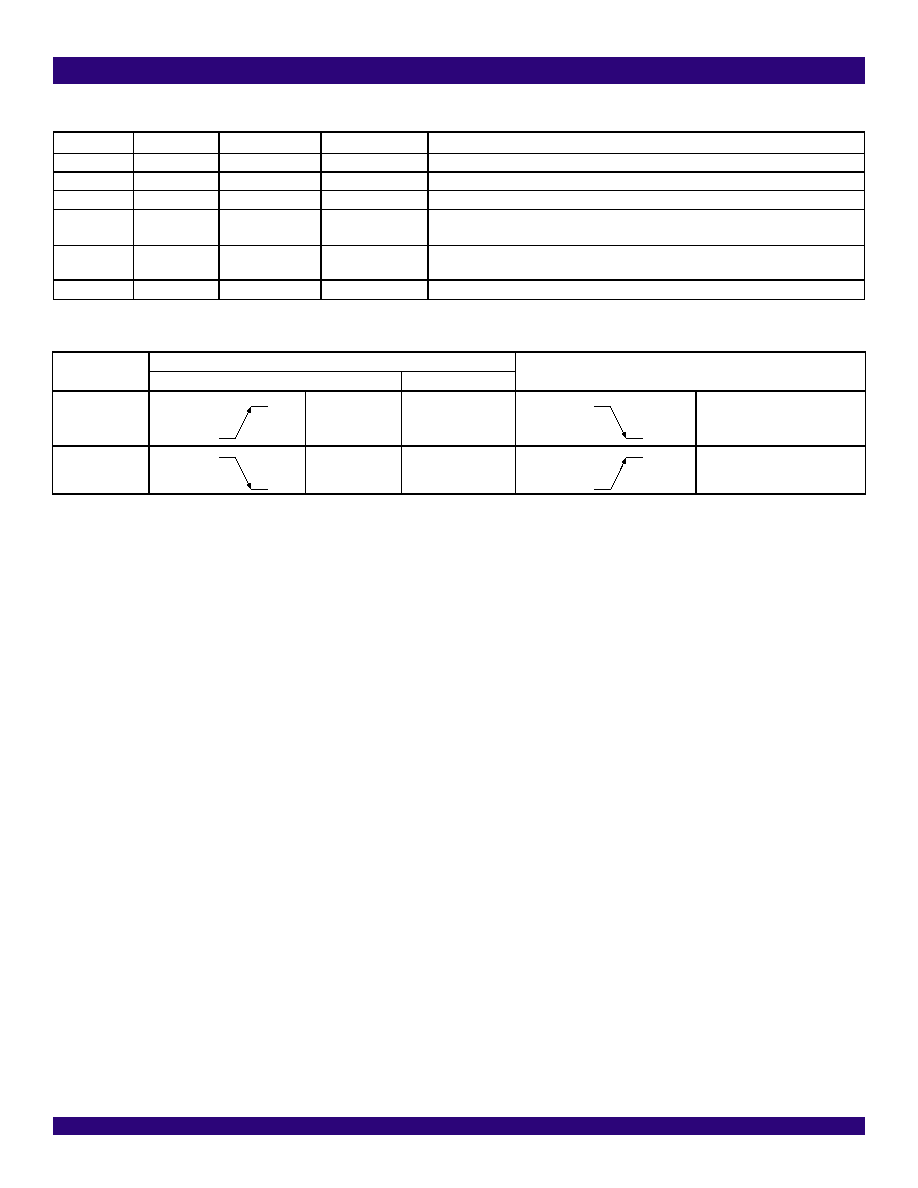
Table-3 System Interface Configuration (In Host Mode)
Pin MCLK
Pin TDNn
CRSn in e-CRS
SINGn in e-SING
Interface
Clocked
High
0
Single Rail Mode 1
Clocked
Pulse
0
1
Single Rail Mode 2
Clocked
Pulse
0
Dual Rail mode with Clock Recovery
Clocked
Pulse
1
0
Dual Rail mode with Data Recovery. Receive just slices the incoming data. Transmit is
determined by the status of TCLKn.
High
Pulse
-
Dual Rail mode with Data Recovery. Receive just slices the incoming data. Transmit is
determined by the status of TCLKn.
Low
Pulse
-
Receiver is powered down. Transmit is determined by the status of TCLKn.
Table-4 Active Clock Edge and Active Level
Pin CLKE
Pin RDn/RDPn and CVn/RDNn
Pin SDO
Clock Recovery
Slicer Output
High
RCLKn
Active High
SCLK
Active High
Low
RCLKn
Active High
Active Low
SCLK
Active High
相关PDF资料 |
PDF描述 |
|---|---|
| IDT72V3640L6BB | IC FIFO SS 1024X36 6NS 144-BGA |
| MS27508E10B35SD | CONN RCPT 13POS BOX MNT W/SCKT |
| IDT82V2048BB | IC LIU T1/E1 8CH SHORT 160-BGA |
| IDT72T3645L6-7BB | IC FIFO 1024X36 6-7NS 208-BGA |
| MAX11208AEUB+T | IC ADC 19BIT SRL 120SPS 10UMAX |
相关代理商/技术参数 |
参数描述 |
|---|---|
| IDT82V2048DA | 功能描述:IC LIU T1/E1 8CH SHORT 144-TQFP RoHS:否 类别:集成电路 (IC) >> 接口 - 驱动器,接收器,收发器 系列:- 标准包装:250 系列:- 类型:收发器 驱动器/接收器数:2/2 规程:RS232 电源电压:3 V ~ 5.5 V 安装类型:表面贴装 封装/外壳:16-TSSOP(0.173",4.40mm 宽) 供应商设备封装:16-TSSOP 包装:带卷 (TR) |
| IDT82V2048DAG | 功能描述:IC LIU T1/E1 8CH SHORT 144-TQFP RoHS:是 类别:集成电路 (IC) >> 接口 - 驱动器,接收器,收发器 系列:- 标准包装:250 系列:- 类型:收发器 驱动器/接收器数:2/2 规程:RS232 电源电压:3 V ~ 5.5 V 安装类型:表面贴装 封装/外壳:16-TSSOP(0.173",4.40mm 宽) 供应商设备封装:16-TSSOP 包装:带卷 (TR) |
| IDT82V2048E | 制造商:IDT 制造商全称:Integrated Device Technology 功能描述:OCTAL CHANNEL T1/E1/J1 SHORT HAUL LINE INTERFACE UNIT |
| IDT82V2048EBB | 功能描述:IC LIU T1/E1 8CH SHORT 208-BGA RoHS:否 类别:集成电路 (IC) >> 接口 - 驱动器,接收器,收发器 系列:- 标准包装:250 系列:- 类型:收发器 驱动器/接收器数:2/2 规程:RS232 电源电压:3 V ~ 5.5 V 安装类型:表面贴装 封装/外壳:16-TSSOP(0.173",4.40mm 宽) 供应商设备封装:16-TSSOP 包装:带卷 (TR) |
| IDT82V2048EBBG | 功能描述:IC LINE INTERFACE UNIT 208-PBGA RoHS:是 类别:集成电路 (IC) >> 接口 - 驱动器,接收器,收发器 系列:- 标准包装:2,500 系列:- 类型:驱动器 驱动器/接收器数:4/0 规程:RS422 电源电压:4.5 V ~ 5.5 V 安装类型:表面贴装 封装/外壳:16-SOIC(0.154",3.90mm 宽) 供应商设备封装:16-SOIC N 包装:带卷 (TR) |
发布紧急采购,3分钟左右您将得到回复。