- 您现在的位置:买卖IC网 > PDF目录1924 > IDT82V2604BBG (IDT, Integrated Device Technology Inc)IC INVERSE MUX 4CH ATM 208-BGA PDF资料下载
参数资料
| 型号: | IDT82V2604BBG |
| 厂商: | IDT, Integrated Device Technology Inc |
| 文件页数: | 5/97页 |
| 文件大小: | 0K |
| 描述: | IC INVERSE MUX 4CH ATM 208-BGA |
| 标准包装: | 1 |
| 应用: | 无线 |
| 接口: | Utopia |
| 电源电压: | 2.97 V ~ 3.63 V |
| 封装/外壳: | 208-BGA |
| 供应商设备封装: | 208-PBGA(17x17) |
| 包装: | 托盘 |
| 安装类型: | 表面贴装 |
| 其它名称: | 82V2604BBG |
第1页第2页第3页第4页当前第5页第6页第7页第8页第9页第10页第11页第12页第13页第14页第15页第16页第17页第18页第19页第20页第21页第22页第23页第24页第25页第26页第27页第28页第29页第30页第31页第32页第33页第34页第35页第36页第37页第38页第39页第40页第41页第42页第43页第44页第45页第46页第47页第48页第49页第50页第51页第52页第53页第54页第55页第56页第57页第58页第59页第60页第61页第62页第63页第64页第65页第66页第67页第68页第69页第70页第71页第72页第73页第74页第75页第76页第77页第78页第79页第80页第81页第82页第83页第84页第85页第86页第87页第88页第89页第90页第91页第92页第93页第94页第95页第96页第97页
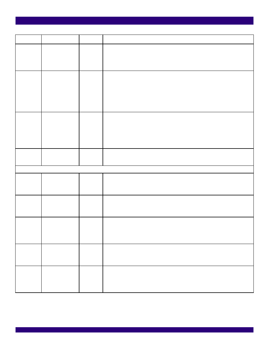
PIN DESCRIPTION
13
December 4, 2006
IDT82V2604
Inverse Multiplexing for ATM
RxAddr4
RxAddr3
RxAddr2
RxAddr1
RxAddr0
C14
C15
C16
D13
D14
I
RxAddr[4:0]: Utopia Receive Address
Utopia receive port address driven from the ATM layer to poll and select an appropriate port.
The RxAddr[4:0] input bus are sampled on the rising edge of RxClk.
RxData7
RxData6
RxData5
RxData4
RxData3
RxData2
RxData1
RxData0
A15
B14
A14
C13
B13
A13
D12
C12
High-Z
O
RxData[7:0]: Utopia Receive Data
Utopia 8-bit data bus driven from the IDT82V2604 to the ATM layer.
The RxData[7:0] output bus are updated on the rising edge of RxClk.
RxClav
B16
High-Z
O
RxClav: Utopia Receive Cell Available
Utopia cell available signal. A polled port drives RxClav only during each cycle following one with its
address on the RxAddr lines. The polled port asserts RxClav high to indicate its corresponding FIFO
has a complete cell available for transfer to the ATM layer, otherwise it deasserts the signal.
The RxClav output is updated on the rising edge of RxClk.
Note: This pin requires a pull-down resistor.
RxSOC
B15
High-Z
O
RxSOC: Utopia Receive Start of Cell
Utopia start of cell pulse. It will be driven high when RxData[7:0] contain the first valid byte of a cell.
The RxSOC input is updated on the rising edge of RxClk.
T1/E1 Line Interface
TSD4
TSD3
TSD2
TSD1
R7
R8
R9
R10
O
TSDn: Transmit Side Data Output
TSDn contains the transmit data for the n-th link.
The TSDn output is updated on the rising edge of TSCKn or TSCCK if common clock is used.
TSCK4
TSCK3
TSCK2
TSCK1
T7
T8
P9
P10
I
TSCKn: Transmit Side Clock
TSCKn contains the transmit clock for the n-th link.
Note: If unused, TSCKn should be connected to ground.
TSF4
TSF3
TSF2
TSF1
P8
T9
T10
T11
I
TSFn: Transmit Side Frame pulse
TSFn is used to delineate each frame for the n-th link.
The TSFn input is sampled on the falling edge of TSCKn or TSCCK if common clock is used.
Note: If unused, TSFn should be connected to ground.
TSCCK
P1
I
TSCCK: Transmit Side Common Clock
TSCCK is the transmit clock for links that are configured in Common Clock Mode.
Note: If unused, TSCCK should be connected to ground.
TSCFS
P2
I
TSCFS: Transmit Side Common Frame Pulse
This signal is used to delineate each frame for links that are configured in Common Clock Mode.
The TSCFS input is sampled on the falling edge of TSCCK.
Note: If unused, TSCFS should be connected to ground.
Table-1 Pin Description (Continued)
Name
Pin Number
Input/Output
Description
相关PDF资料 |
PDF描述 |
|---|---|
| IDT82V2608BBG | IC INVERSE MUX 8CH ATM 208-BGA |
| IDT82V2616BBG | IC INVERSE MUX 16CH ATM 272-PBGA |
| IDT88K8483BRI | IC SPI-4 EXCHANGE 3PORT 672-BGA |
| IDT88P8341BHI | IC SPI3-SPI4 EXCHANGE 820-PBGA |
| IDT88P8342BHI | IC SPI3-SPI4 EXCHANGE 820-PBGA |
相关代理商/技术参数 |
参数描述 |
|---|---|
| IDT82V2608 | 制造商:IDT 制造商全称:Integrated Device Technology 功能描述:INVERSE MULTIPLEXING FOR ATM |
| IDT82V2608BB | 功能描述:IC INVERSE MUX 8CH ATM 208-BGA RoHS:否 类别:集成电路 (IC) >> 接口 - 专用 系列:- 标准包装:3,000 系列:- 应用:PDA,便携式音频/视频,智能电话 接口:I²C,2 线串口 电源电压:1.65 V ~ 3.6 V 封装/外壳:24-WQFN 裸露焊盘 供应商设备封装:24-QFN 裸露焊盘(4x4) 包装:带卷 (TR) 安装类型:表面贴装 产品目录页面:1015 (CN2011-ZH PDF) 其它名称:296-25223-2 |
| IDT82V2608BBG | 功能描述:IC INVERSE MUX 8CH ATM 208-BGA RoHS:是 类别:集成电路 (IC) >> 接口 - 专用 系列:- 标准包装:3,000 系列:- 应用:PDA,便携式音频/视频,智能电话 接口:I²C,2 线串口 电源电压:1.65 V ~ 3.6 V 封装/外壳:24-WQFN 裸露焊盘 供应商设备封装:24-QFN 裸露焊盘(4x4) 包装:带卷 (TR) 安装类型:表面贴装 产品目录页面:1015 (CN2011-ZH PDF) 其它名称:296-25223-2 |
| IDT82V2616 | 制造商:IDT 制造商全称:Integrated Device Technology 功能描述:INVERSE MULTIPLEXING FOR ATM |
| IDT82V2616BB | 功能描述:IC INVERSE MUX 16CH ATM 272-PBGA RoHS:否 类别:集成电路 (IC) >> 接口 - 专用 系列:- 标准包装:3,000 系列:- 应用:PDA,便携式音频/视频,智能电话 接口:I²C,2 线串口 电源电压:1.65 V ~ 3.6 V 封装/外壳:24-WQFN 裸露焊盘 供应商设备封装:24-QFN 裸露焊盘(4x4) 包装:带卷 (TR) 安装类型:表面贴装 产品目录页面:1015 (CN2011-ZH PDF) 其它名称:296-25223-2 |
发布紧急采购,3分钟左右您将得到回复。