- 您现在的位置:买卖IC网 > PDF目录67716 > IDT8737-11PGI8 (INTEGRATED DEVICE TECHNOLOGY INC) 8737 SERIES, LOW SKEW CLOCK DRIVER, 4 TRUE OUTPUT(S), 0 INVERTED OUTPUT(S), PDSO20 PDF资料下载
参数资料
| 型号: | IDT8737-11PGI8 |
| 厂商: | INTEGRATED DEVICE TECHNOLOGY INC |
| 元件分类: | 时钟及定时 |
| 英文描述: | 8737 SERIES, LOW SKEW CLOCK DRIVER, 4 TRUE OUTPUT(S), 0 INVERTED OUTPUT(S), PDSO20 |
| 封装: | TSSOP-20 |
| 文件页数: | 2/12页 |
| 文件大小: | 98K |
| 代理商: | IDT8737-11PGI8 |
10
COMMERCIALANDINDUSTRIALTEMPERATURERANGES
IDT8737-11
LOW SKEW,
÷÷÷÷÷1/÷÷÷÷÷2 DIFFERENTIAL-TO-3.3V LVPECL
POWER CONSIDERATIONS
This section provides information on power dissipation and junction temperature for the IDT8737-11. Equations and example calculations are also provided.
POWER DISSIPATION:
The total power dissipation for the IDT8737-11 is the sum of the core power plus the power dissipated in the load(s). The following is the power dissipation
for the VDD = 3.3V + 5% = 3.465V, which gives worst case results. Please refer to the following section, Calculations and Equations, for details on calculating
power dissipated in the load.
Power (core)MAX = VDD_MAX * ICC_MAX = 3.465 * 55mA = 190.57mW
Power (outputs)MAX = 30.2mW/Loaded Output Pair
If all outputs are loaded, the total power is 4 * 30.2mW = 120.8mW
Total Power_MAX (3.465V, with all outputs switching) = 190.57mW + 120.8mW = 311.37mW
JUNCTION TEMPERATURE:
Junction temperature (tJ) is the temperature at the junction of the bond wire and bond pad. It directly affects the reliability of the device. The maximum
recommended junction temperature for this device is 125°C.
The equation for is as follows: tJ =
θJA * Pd_total + TA
tJ = Junction Temperature
θJA=Junction-to-AmbientThermalResistance
Pd_total = Total Device Power Dissipation (example calculation is in Power Dissipation, above)
TA = Ambient Temperature
In order to calculate junction temperature, the appropriate junction-to-ambient thermal resistance (
θJA)mustbeused. Assumingamoderateairflowof200
linear feet per minute and a multi-layer board, the appropriate value is 77.6°C/W per the following Thermal Resistance table. Therefore, tJ for an ambient
temperature of 85°C with all its outputs switching is:
85°C + 0.311W * 77.6°C/W = 109.16°C. This is well below the limit of 125°C.
This calculation is only an example. tJ will obviously vary depending on the number of loaded outputs, supply voltage, air flow, and the type of board (single-
layer or multi-layer).
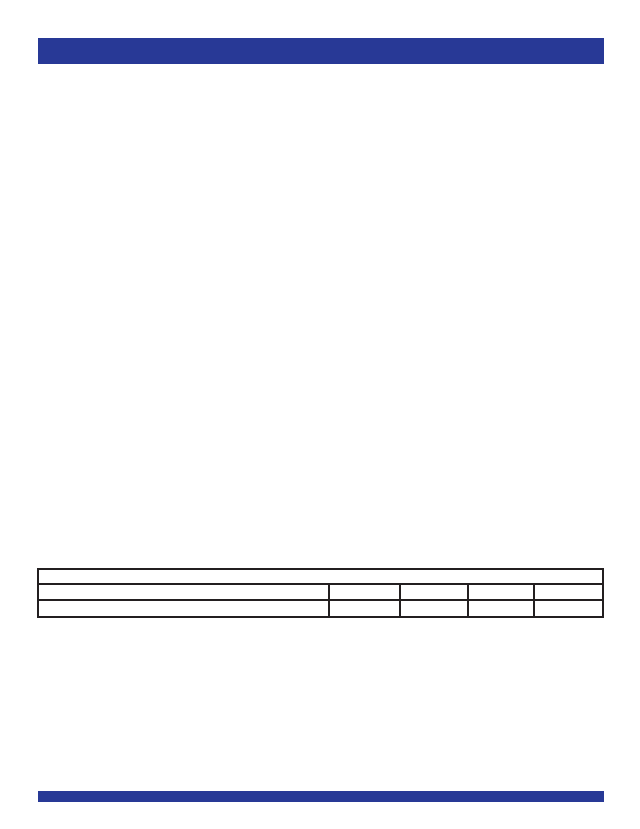
THERMALRESISTANCE
θJA for 20-pin TSSOP, forced convection
θθθθθJA by Velocity (Linear Feet per mInute)
0
200
400
Unit
Multi-Layer PCB, JEDEC Standard Test boards
92.6
77.6
70.9
°C/W
相关PDF资料 |
PDF描述 |
|---|---|
| IDTCSPT857BV8 | CSPT857 SERIES, PLL BASED CLOCK DRIVER, 10 TRUE OUTPUT(S), 0 INVERTED OUTPUT(S), BGA56 |
| IDTCSPT857PA8 | CSPT857 SERIES, PLL BASED CLOCK DRIVER, 10 TRUE OUTPUT(S), 0 INVERTED OUTPUT(S), PDSO48 |
| IDTCSPT857CBVG8 | PLL BASED CLOCK DRIVER, 10 TRUE OUTPUT(S), 0 INVERTED OUTPUT(S), PBGA56 |
| IDTCSPT857CNL8 | 857 SERIES, PLL BASED CLOCK DRIVER, 10 TRUE OUTPUT(S), 0 INVERTED OUTPUT(S), QCC40 |
| IDTCSPT857CPAI8 | 857 SERIES, PLL BASED CLOCK DRIVER, 10 TRUE OUTPUT(S), 0 INVERTED OUTPUT(S), PDSO48 |
相关代理商/技术参数 |
参数描述 |
|---|---|
| IDT88K8483BRI | 功能描述:IC SPI-4 EXCHANGE 3PORT 672-BGA RoHS:否 类别:集成电路 (IC) >> 专用 IC 系列:* 产品培训模块:Lead (SnPb) Finish for COTS Obsolescence Mitigation Program 标准包装:1 系列:- 类型:调帧器 应用:数据传输 安装类型:表面贴装 封装/外壳:400-BBGA 供应商设备封装:400-PBGA(27x27) 包装:散装 |
| IDT88P8341BHGI | 功能描述:IC SPI3-SPI4 EXCHANGE 820-PBGA RoHS:是 类别:集成电路 (IC) >> 专用 IC 系列:* 产品培训模块:Lead (SnPb) Finish for COTS Obsolescence Mitigation Program 标准包装:1 系列:- 类型:调帧器 应用:数据传输 安装类型:表面贴装 封装/外壳:400-BBGA 供应商设备封装:400-PBGA(27x27) 包装:散装 |
| IDT88P8341BHI | 功能描述:IC SPI3-SPI4 EXCHANGE 820-PBGA RoHS:否 类别:集成电路 (IC) >> 专用 IC 系列:* 产品培训模块:Lead (SnPb) Finish for COTS Obsolescence Mitigation Program 标准包装:1 系列:- 类型:调帧器 应用:数据传输 安装类型:表面贴装 封装/外壳:400-BBGA 供应商设备封装:400-PBGA(27x27) 包装:散装 |
| IDT88P8342BHGI | 功能描述:IC SPI3-SPI4 EXCHANGE 820-PBGA RoHS:是 类别:集成电路 (IC) >> 专用 IC 系列:* 产品培训模块:Lead (SnPb) Finish for COTS Obsolescence Mitigation Program 标准包装:1 系列:- 类型:调帧器 应用:数据传输 安装类型:表面贴装 封装/外壳:400-BBGA 供应商设备封装:400-PBGA(27x27) 包装:散装 |
| IDT88P8342BHI | 功能描述:IC SPI3-SPI4 EXCHANGE 820-PBGA RoHS:否 类别:集成电路 (IC) >> 专用 IC 系列:* 产品培训模块:Lead (SnPb) Finish for COTS Obsolescence Mitigation Program 标准包装:1 系列:- 类型:调帧器 应用:数据传输 安装类型:表面贴装 封装/外壳:400-BBGA 供应商设备封装:400-PBGA(27x27) 包装:散装 |
发布紧急采购,3分钟左右您将得到回复。