- 您现在的位置:买卖IC网 > PDF目录67123 > IMISC660EYB (CYPRESS SEMICONDUCTOR CORP) LOW SKEW CLOCK DRIVER, PDSO28 PDF资料下载
参数资料
| 型号: | IMISC660EYB |
| 厂商: | CYPRESS SEMICONDUCTOR CORP |
| 元件分类: | 时钟及定时 |
| 英文描述: | LOW SKEW CLOCK DRIVER, PDSO28 |
| 封装: | SSOP-28 |
| 文件页数: | 2/7页 |
| 文件大小: | 54K |
| 代理商: | IMISC660EYB |
SC660E
I
2C System Clock Buffer for Mobile Applications
Approved Product
INTERNATIONAL MICROCIRCUITS, INC. 525 LOS COCHES ST.
Rev.2.5
2/17/2000
MILPITAS, CA 95035. TEL: 408-263-6300. FAX 408-263-6571
Page 2 of 7
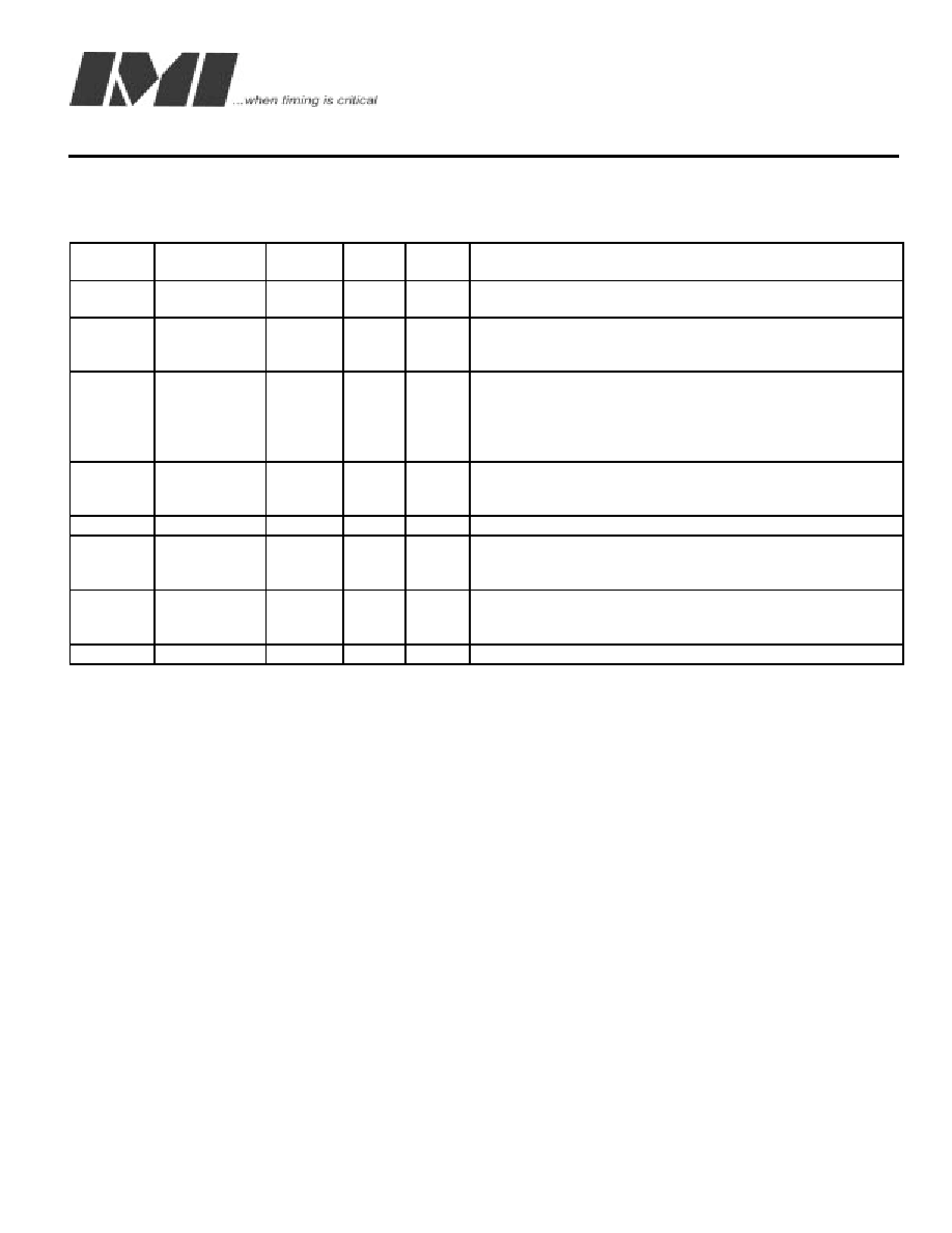
Pin Description
PIN
No.
Pin
Name
PWR
I/O
TYPE
Description
9
FIN
-
I
PAD
This pin is connected to the input reference clock. This clock
must be in the range of 10.0 to 100.0 Mhz.
2,3,6,7,1
1,18,22,2
3,26,27
SDRAM(0:9)
VDDB
O
BUF1
Low skew output clocks .
20
OE
-
I
PAD
Buffer Output Enable pin. This pin is low it is used to place
all output clocks (CLK1:10) in a tri state condition. This
feature facilitates in production board level testing to be
easily implemented for the clocks that this device produces.
Has internal pull-up resistor.
14
SDATA
VDD
I/O
PAD
Serial Data for I2C control interface. This pin receives data
streams from the I2C bus and outputs an acknowledge for
valid data.
15
SCLOCK
VDD
I
PAD
Serial Clock for I2C control interface.
4, 8, 12,
16, 17,
21, 25
VSS
PWR
-
Ground pins for clock output buffers. These pins must be
returned to the same potential to reduce output clock skew.
1, 5, 10,
19, 24,
28
VDDB
-
PWR
-
Power for output clock buffers.
13
VDD
-
PWR
-
Pin for device core logic.
Maximum Ratings
Voltage Relative to VSS:
-0.3V
Voltage Relative to VDD:
0.3V
Storage Temperature:
-65C to + 150C
Operating Temperature:
-40C to +85C
Maximum Power Supply:
7V
This device contains circuitry to protect the inputs
against damage due to high static voltages or electric
field; however, precautions should be taken to avoid
application of any voltage higher than the maximum
rated voltages to this circuit. For proper operation, Vin
and Vout should be constrained to the range:
VSS<(Vin or Vout)<VDD
Unused inputs must always be tied to an appropriate
logic voltage level (either VSS or VDD).
相关PDF资料 |
PDF描述 |
|---|---|
| IMISC680CYB | LOW SKEW CLOCK DRIVER, PDSO48 |
| IMISG508APB | 40 MHz, PROC SPECIFIC CLOCK GENERATOR, PDIP16 |
| IMISG509APB | 60 MHz, PROC SPECIFIC CLOCK GENERATOR, PDIP16 |
| IMSB409-1 | SPECIALTY MICROPROCESSOR CIRCUIT, DMA16 |
| IMSB430-10 | SPECIALTY MICROPROCESSOR CIRCUIT, XMA |
相关代理商/技术参数 |
参数描述 |
|---|---|
| IMISC670DYB | 制造商:未知厂家 制造商全称:未知厂家 功能描述:CPU System Clock Generator |
| IMISC671CTB | 制造商:未知厂家 制造商全称:未知厂家 功能描述:CPU System Clock Generator |
| IMISC671CYB | 制造商:未知厂家 制造商全称:未知厂家 功能描述:CPU System Clock Generator |
| IMISC671DYB | 制造商:未知厂家 制造商全称:未知厂家 功能描述:CPU System Clock Generator |
| IMISC674BYB | 制造商:未知厂家 制造商全称:未知厂家 功能描述:CPU System Clock Generator |
发布紧急采购,3分钟左右您将得到回复。