参数资料
| 型号: | IP80C88-2 |
| 厂商: | Intersil |
| 文件页数: | 38/38页 |
| 文件大小: | 0K |
| 描述: | IC CPU 8/16BIT 5V 8MHZ 40-DIP |
| 标准包装: | 99 |
| 处理器类型: | 80C88 8/16-位 |
| 速度: | 8MHz |
| 电压: | 4.75 V ~ 5.25 V |
| 安装类型: | 通孔 |
| 封装/外壳: | 40-DIP(0.600",15.24mm) |
| 供应商设备封装: | 40-DIP |
| 包装: | 管件 |
第1页第2页第3页第4页第5页第6页第7页第8页第9页第10页第11页第12页第13页第14页第15页第16页第17页第18页第19页第20页第21页第22页第23页第24页第25页第26页第27页第28页第29页第30页第31页第32页第33页第34页第35页第36页第37页当前第38页
9
FN2949.4
February 22, 2008
Bus Operation
The 80C88 address/data bus is broken into three parts: the
lower eight address/data bits (AD0-AD7), the middle eight
address bits (A8-A15), and the upper four address bits (A16-
A19). The address/data bits and the highest four address
bits are time multiplexed. This technique provides the most
efficient use of pins on the processor, permitting the use of
standard 40 lead package. The middle eight address bits are
not multiplexed, i.e., they remain valid throughout each bus
cycle. In addition, the bus can be demultiplexed at the
processor with a single address latch if a standard, non
multiplexed bus is desired for the system.
Each processor bus cycle consists of at least four CLK
cycles. These are referred to as T1, T2, T3 and T4. (See
Figure 5). The address is emitted from the processor during
T1 and data transfer occurs on the bus during T3 and T4. T2
is used primarily for changing the direction of the bus during
read operations. In the event that a “Not Ready” indication is
given by the addressed device, “wait” states (TW) are
inserted between T3 and T4. Each inserted “wait” state is of
the same duration as a CLK cycle. Periods can occur
between 80C88 driven bus cycles. These are referred to as
“idle” states (TI), or inactive CLK cycles. The processor uses
these cycles for internal housekeeping.
During T1 of any bus cycle, the ALE (Address latch enable)
signal is emitted (by either the processor or the 82C88 bus
controller, depending on the MN/MX strap). At the trailing
edge of this pulse, a valid address and certain status
information for the cycle may be latched.
Status bits S0, S1, and S2 are used by the bus controller, in
maximum mode, to identify the type of bus transaction
according to Table 2.
Status bits S3 through S6 are multiplexed with high order
address bits and are therefore valid during T2 through T4.
S3 and S4 indicate which segment register was used to this
bus cycle in forming the address according to Table 3.
S5 is a reflection of the PSW interrupt enable bit. S6 is
always equal to 0.
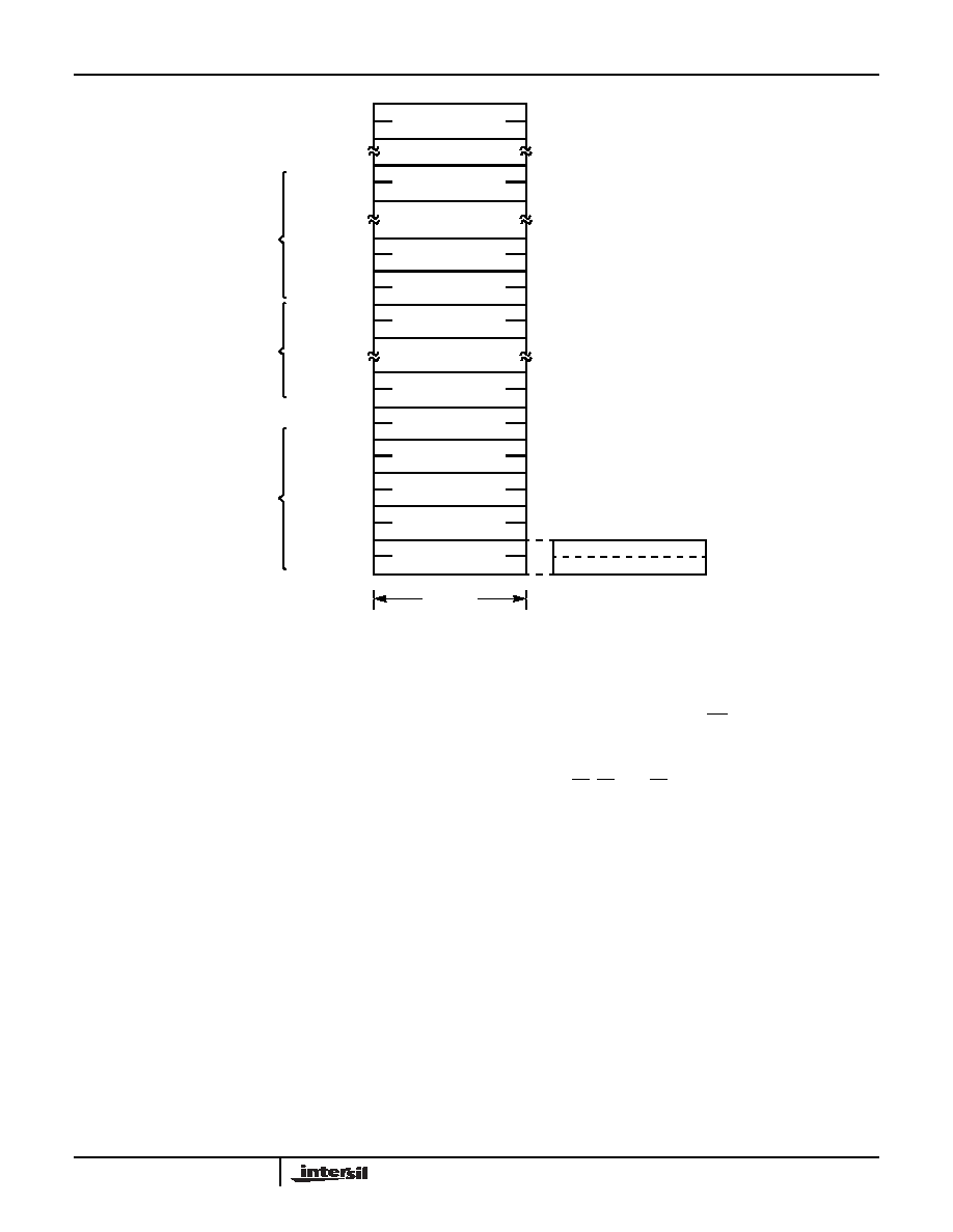
TYPE 255 POINTER
(AVAILABLE)
RESET BOOTSTRAP
PROGRAM JUMP
TYPE 33 POINTER
(AVAILABLE)
TYPE 32 POINTER
(AVAILABLE)
TYPE 31 POINTER
(AVAILABLE)
TYPE 5 POINTER
(RESERVED)
TYPE 4 POINTER
OVERFLOW
TYPE 3 POINTER
1 BYTE INT INSTRUCTION
TYPE 2 POINTER
NON MASKABLE
TYPE 1 POINTER
SINGLE STEP
TYPE 0 POINTER
DIVIDE ERROR
CS BASE ADDRESS
IP OFFSET
014H
010H
00CH
008H
004H
000H
07FH
080H
084H
FFFF0H
FFFFFH
3FFH
3FCH
AVAILABLE
INTERRUPT
POINTERS
(224)
DEDICATED
INTERRUPT
POINTERS
(5)
RESERVED
INTERRUPT
POINTERS
(27)
FIGURE 2. RESERVED MEMORY LOCATIONS
16-BITS
80C88
相关PDF资料 |
PDF描述 |
|---|---|
| IS80C286-20 | IC CPU 16BIT 5V 20MHZ 68-PLCC |
| ISL1532IRZ | IC LINE DRIVER DUAL 24-QFN |
| ISL1536IRZ | IC LINE DRVR DUAL ADSL2+ 16-QFN |
| ISL1539AIRZ | IC VDSL2 LINE DVR AMP 24QFN |
| ISL1539IVEZ | IC VDSL2 LINE DVR AMP 24HTTSOP |
相关代理商/技术参数 |
参数描述 |
|---|---|
| IP80C88-2/+ | 制造商:未知厂家 制造商全称:未知厂家 功能描述:16-Bit Microprocessor |
| IP80C88-2S2064 | 制造商:Rochester Electronics LLC 功能描述:- Bulk |
| IP80C88S2064 | 制造商:Rochester Electronics LLC 功能描述:- Bulk |
| IP8101-032 | 制造商:SMC Corporation of America 功能描述:POSITIONER |
| IP8101-032-DH | 制造商:SMC Corporation of America 功能描述:Positioner, IP8000/8100 |
发布紧急采购,3分钟左右您将得到回复。