- 您现在的位置:买卖IC网 > Datasheet目录445 > IRFL1006TR (International Rectifier)MOSFET N-CH 60V 1.6A SOT223 Datasheet资料下载
参数资料
| 型号: | IRFL1006TR |
| 厂商: | International Rectifier |
| 文件页数: | 2/9页 |
| 文件大小: | 0K |
| 描述: | MOSFET N-CH 60V 1.6A SOT223 |
| 标准包装: | 2,500 |
| 系列: | HEXFET® |
| FET 型: | MOSFET N 通道,金属氧化物 |
| FET 特点: | 标准 |
| 漏极至源极电压(Vdss): | 60V |
| 电流 - 连续漏极(Id) @ 25° C: | 1.6A |
| 开态Rds(最大)@ Id, Vgs @ 25° C: | 220 毫欧 @ 1.6A,10V |
| Id 时的 Vgs(th)(最大): | 4V @ 250µA |
| 闸电荷(Qg) @ Vgs: | 8nC @ 10V |
| 输入电容 (Ciss) @ Vds: | 160pF @ 25V |
| 功率 - 最大: | 1W |
| 安装类型: | 表面贴装 |
| 封装/外壳: | TO-261-4,TO-261AA |
| 供应商设备封装: | SOT-223 |
| 包装: | 带卷 (TR) |
�� �
�
�IRFL1006�
�Electrical� Characteristics� @� T� J� =� 25°C� (unless� otherwise� specified)�
�Parameter�
�Min.� Typ.� Max.� Units�
�Conditions�
�V� (BR)DSS�
�Drain-to-Source� Breakdown� Voltage�
�60� –––� –––� V� V� GS� =� 0V,� I� D� =� 250μA�
�?� V� (BR)DSS� /� ?� T� J�
�R� DS(on)�
�Breakdown� Voltage� Temp.� Coefficient�
�Static� Drain-to-Source� On-Resistance�
�–––� 0.057� –––�
�–––� –––� 0.22�
�V/°C�
�?�
�Reference� to� 25°C,� I� D� =� 1mA�
�V� GS� =� 10V,� I� D� =� 1.6A� ?�
�–––� 18� –––� R� G� =� 49� ?�
�V� GS(th)�
�g� fs�
�I� DSS�
�I� GSS�
�Q� g�
�Q� gs�
�Q� gd�
�t� d(on)�
�t� r�
�t� d(off)�
�t� f�
�C� iss�
�C� oss�
�C� rss�
�Gate� Threshold� Voltage�
�Forward� Transconductance�
�Drain-to-Source� Leakage� Current�
�Gate-to-Source� Forward� Leakage�
�Gate-to-Source� Reverse� Leakage�
�Total� Gate� Charge�
�Gate-to-Source� Charge�
�Gate-to-Drain� ("Miller")� Charge�
�Turn-On� Delay� Time�
�Rise� Time�
�Turn-Off� Delay� Time�
�Fall� Time�
�Input� Capacitance�
�Output� Capacitance�
�Reverse� Transfer� Capacitance�
�2.0� –––� 4.0� V� V� DS� =� V� GS� ,� I� D� =� 250μA�
�3.0� –––� –––� S� V� DS� =� 25V,� I� D� =� 1.6A�
�–––� –––� 25� V� DS� =� 60V,� V� GS� =� 0V�
�μA�
�–––� –––� 250� V� DS� =� 48V,� V� GS� =� 0V,� T� J� =� 125°C�
�–––� –––� 100� V� GS� =� 20V�
�nA�
�–––� –––� -100� V� GS� =� -20V�
�–––� –––� 8.0� I� D� =� 1.6A�
�–––� –––� 1.7� nC� V� DS� =� 48V�
�–––� –––� 3.3� V� GS� =� 10V,� See� Fig.� 6� and� 9� ?�
�–––� 7.4� –––� V� DD� =� 30V�
�–––� 18� –––� I� D� =� 1.6A�
�ns�
�–––� 17� –––� R� D� =� 19� ?� ,� See� Fig.� 10� ?�
�–––� 160� –––� V� GS� =� 0V�
�–––� 55� –––� pF� V� DS� =� 25V�
�–––� 19� –––� ?� =� 1.0MHz,� See� Fig.� 5�
�Source-Drain� Ratings� and� Characteristics�
�Parameter�
�Min.� Typ.� Max.� Units�
�Conditions�
�I� S�
�I� SM�
�Continuous� Source� Current�
�(Body� Diode)�
�Pulsed� Source� Current�
�(Body� Diode)� ?�
�–––� –––� 1.6�
�–––� –––� 6.4�
�A�
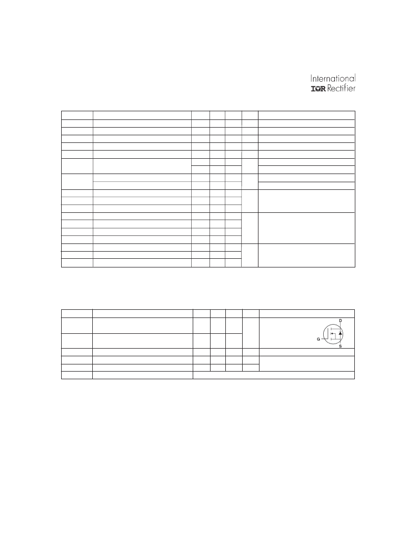
�MOSFET� symbol�
�showing� the�
�integral� reverse�
�p-n� junction� diode.�
�V� SD�
�t� rr�
�Q� rr�
�t� on�
�Notes:�
�Diode� Forward� Voltage�
�Reverse� Recovery� Time�
�Reverse� RecoveryCharge�
�Forward� Turn-On� Time�
�–––� –––� 1.3� V� T� J� =� 25°C,� I� S� =� 1.6A,� V� GS� =� 0V� ?�
�–––� 31� 47� ns� T� J� =� 25°C,� I� F� =� 1.6A�
�–––� 46� 68� nC� di/dt� =� 100A/μs� ?�
�Intrinsic� turn-on� time� is� negligible� (turn-on� is� dominated� by� L� S� +L� D� )�
�?� Repetitive� rating;� pulse� width� limited� by�
�max.� junction� temperature.� (� See� fig.� 11� )�
�?� Starting� T� J� =� 25°C,� L� =� 42� mH�
�R� G� =� 25� ?� ,� I� AS� =� 1.6A.� (See� Figure� 12)�
�2�
�?� I� SD� ≤� 1.6A,� di/dt� ≤� 260A/μs,� V� DD� ≤� V� (BR)DSS� ,�
�T� J� ≤� 150°C�
�?� Pulse� width� ≤� 300μs;� duty� cycle� ≤� 2%.�
�www.irf.com�
�相关PDF资料 |
PDF描述 |
|---|---|
| IRFL4105PBF | MOSFET N-CH 55V 3.7A SOT223 |
| IRFL4105 | MOSFET N-CH 55V 3.7A SOT223 |
| IRFL4310TR | MOSFET N-CH 100V 1.6A SOT223 |
| IRFM120ATF | MOSFET N-CH 100V 2.3A SOT-223 |
| IRFP044N | MOSFET N-CH 55V 53A TO-247AC |
相关代理商/技术参数 |
参数描述 |
|---|---|
| IRFL110 | 功能描述:MOSFET N-Chan 100V 1.5 Amp RoHS:否 制造商:STMicroelectronics 晶体管极性:N-Channel 汲极/源极击穿电压:650 V 闸/源击穿电压:25 V 漏极连续电流:130 A 电阻汲极/源极 RDS(导通):0.014 Ohms 配置:Single 最大工作温度: 安装风格:Through Hole 封装 / 箱体:Max247 封装:Tube |
| IRFL110PBF | 功能描述:MOSFET N-Chan 100V 1.5 Amp RoHS:否 制造商:STMicroelectronics 晶体管极性:N-Channel 汲极/源极击穿电压:650 V 闸/源击穿电压:25 V 漏极连续电流:130 A 电阻汲极/源极 RDS(导通):0.014 Ohms 配置:Single 最大工作温度: 安装风格:Through Hole 封装 / 箱体:Max247 封装:Tube |
| IRFL110TR | 功能描述:MOSFET N-Chan 100V 1.5 Amp RoHS:否 制造商:STMicroelectronics 晶体管极性:N-Channel 汲极/源极击穿电压:650 V 闸/源击穿电压:25 V 漏极连续电流:130 A 电阻汲极/源极 RDS(导通):0.014 Ohms 配置:Single 最大工作温度: 安装风格:Through Hole 封装 / 箱体:Max247 封装:Tube |
| IRFL110TRPBF | 功能描述:MOSFET N-Chan 100V 1.5 Amp RoHS:否 制造商:STMicroelectronics 晶体管极性:N-Channel 汲极/源极击穿电压:650 V 闸/源击穿电压:25 V 漏极连续电流:130 A 电阻汲极/源极 RDS(导通):0.014 Ohms 配置:Single 最大工作温度: 安装风格:Through Hole 封装 / 箱体:Max247 封装:Tube |
| IRFL210 | 功能描述:MOSFET N-Chan 200V 0.96 Amp RoHS:否 制造商:STMicroelectronics 晶体管极性:N-Channel 汲极/源极击穿电压:650 V 闸/源击穿电压:25 V 漏极连续电流:130 A 电阻汲极/源极 RDS(导通):0.014 Ohms 配置:Single 最大工作温度: 安装风格:Through Hole 封装 / 箱体:Max247 封装:Tube |
发布紧急采购,3分钟左右您将得到回复。