- 您现在的位置:买卖IC网 > PDF目录377521 > IRHM57264SE (International Rectifier) Thru-Hole Radiation Hardened Power MOSFET(通孔安装抗辐射功率MOSFET) PDF资料下载
参数资料
| 型号: | IRHM57264SE |
| 厂商: | International Rectifier |
| 英文描述: | Thru-Hole Radiation Hardened Power MOSFET(通孔安装抗辐射功率MOSFET) |
| 中文描述: | 通孔抗辐射功率MOSFET(通孔安装抗辐射功率MOSFET的) |
| 文件页数: | 3/8页 |
| 文件大小: | 94K |
| 代理商: | IRHM57264SE |
www.irf.com
3
Radiation Characteristics
IRHM57264SE
International Rectifier Radiation Hardened MOSFETs are tested to verify their radiation hardness capability.
The hardness assurance program at International Rectifier is comprised of two radiation environments.
Every manufacturing lot is tested for total ionizing dose (per notes 5 and 6) using the TO-3 package. Both
pre- and post-irradiation performance are tested and specified using the same drive circuitry and test
conditions in order to provide a direct comparison.
1. Part number IRHM57264SE
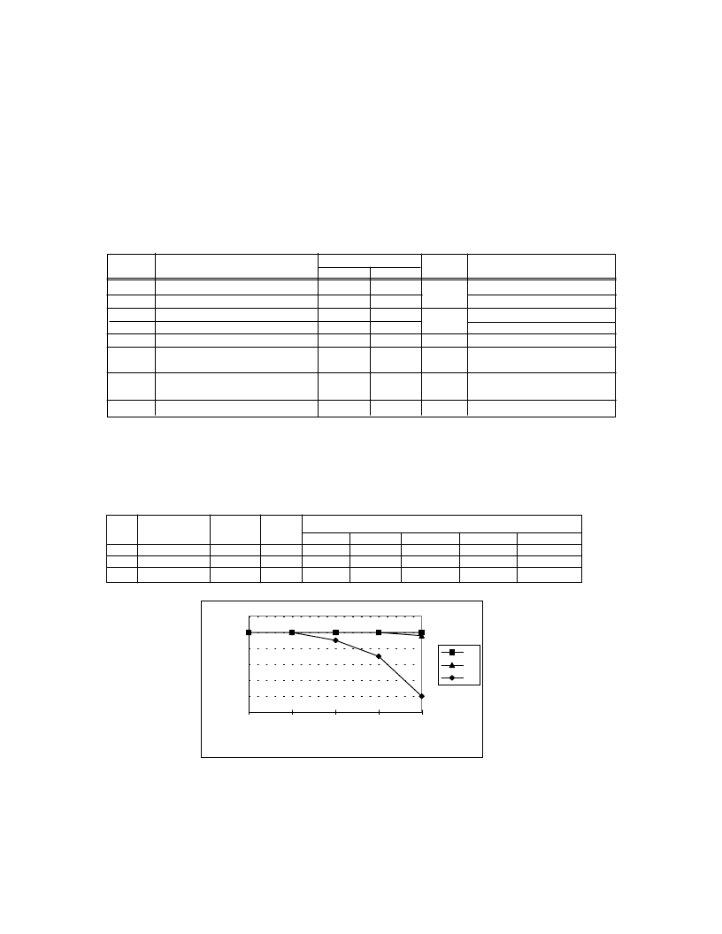
Fig a.
Single Event Effect, Safe Operating Area
International Rectifier radiation hardened MOSFETs have been characterized in heavy ion environment for
Single Event Effects (SEE). Single Event Effects characterization is illustrated in Fig. a and Table 2.
For footnotes refer to the last page
Table 2. Single Event Effect Safe Operating Area
Ion
MeV/(mg/cm
2
)) (MeV) (μm)
@VGS=0V@VGS=-5V @VGS=-10V @VGS=-15V @VGS=-20V
Br
36.7
309 39.5 250 250 250 250 250
I
59.8
341 32.5 250 250 250 250 240
Au
82.3
350 28.4 250 250 225 175
LET
Energy Range
VDS (V)
50
0
50
100
150
200
250
300
0
-5
-10
-15
-20
VGS
V
Br
I
Au
Table 1. Electrical Characteristics @ Tj = 25°C, Post Total Dose Irradiation
Parameter
100K Rads (Si)
Min
250
2.0
—
—
—
Units
Test Conditions
Max
—
4.5
100
-100
10
BV
DSS
V
GS(th)
I
GSS
I
GSS
I
DSS
R
DS(on)
Drain-to-Source Breakdown Voltage
Gate Threshold Voltage
Gate-to-Source Leakage Forward
Gate-to-Source Leakage Reverse
Zero Gate Voltage Drain Current
Static Drain-to-Source
On-State Resistance (TO-3)
Static Drain-to-Source
On-State Resistance (TO-254)
V
V
GS
= 0V, I
D
= 1.0mA
V
GS
= V
DS
, I
D
= 1.0mA
V
GS
= 20V
V
GS
= -20V
V
DS
=160V, V
GS
=0V
nA
μA
—
0.061
V
GS
= 12V, I
D
= 35A
R
DS(on)
V
SD
Diode Forward Voltage
—
1.2
V
V
GS
= 0V, I
D
= 35A
— 0.066
V
GS
= 12V, I
D
= 35A
相关PDF资料 |
PDF描述 |
|---|---|
| IRHM7054 | HEXFET Transistor(HEXFET 晶体管) |
| IRHM8054 | HEXFET Transistor(HEXFET 晶体管) |
| IRHM7160 | HEXFET Transistor(HEXFET 晶体管) |
| IRHM9130 | P-Channel RAD HARD HEXFET TRANSISTOR(P 沟道 Rad Hard 技术 HEXFET晶体管) |
| IRHM93160 | HEXFET Transistor(HEXFET 晶体管) |
相关代理商/技术参数 |
参数描述 |
|---|---|
| IRHM57264SESCS | 制造商:International Rectifier 功能描述:HIREL, HEXFET RHD - Bulk |
| IRHM57264SESCV | 制造商:International Rectifier 功能描述:HIREL, HEXFET RHD - Bulk |
| IRHM57Z60 | 制造商:International Rectifier 功能描述:MOSFET, HIREL, RAD HARD, R5 - Bulk |
| IRHM57Z60SCS | 制造商:International Rectifier 功能描述:HIREL, HEXFET RHD - Bulk |
| IRHM57Z60SCV | 制造商:International Rectifier 功能描述:HIREL, HEXFET RHD - Bulk |
发布紧急采购,3分钟左右您将得到回复。