- 您现在的位置:买卖IC网 > PDF目录360969 > IRLBL1304 TRANSISTOR | MOSFET | N-CHANNEL | 40V V(BR)DSS | 95A I(D) | TO-263AA PDF资料下载
参数资料
| 型号: | IRLBL1304 |
| 英文描述: | TRANSISTOR | MOSFET | N-CHANNEL | 40V V(BR)DSS | 95A I(D) | TO-263AA |
| 中文描述: | 晶体管| MOSFET的| N沟道| 40V的五(巴西)直| 95A章一(d)|对263AA |
| 文件页数: | 2/8页 |
| 文件大小: | 215K |
| 代理商: | IRLBL1304 |
IRLBL1304
2
www.irf.com
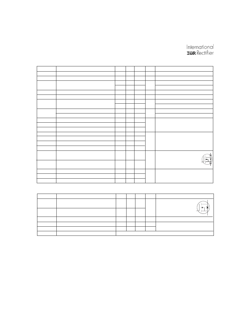
Parameter
Min.
40
–––
–––
–––
1.0
120
–––
–––
–––
–––
–––
–––
–––
–––
–––
–––
–––
Typ. Max. Units
–––
–––
0.043 –––
––– 0.0045
––– 0.0065
–––
–––
–––
–––
–––
25
–––
250
–––
100
–––
-100
–––
140
–––
39
–––
79
21
–––
350
–––
45
–––
103
–––
Conditions
V
GS
= 0V, I
D
= 250μA
Reference to 25°C, I
D
= 1mA
V
GS
= 10V, I
D
= 110A
V
GS
= 4.5V, I
D
= 93
V
DS
= V
GS
, I
D
= 250μA
V
DS
= 25V, I
D
= 110A
V
DS
= 40V, V
GS
= 0V
V
DS
= 32V, V
GS
= 0V, T
J
= 150°C
V
GS
= 16V
V
GS
= -16V
I
D
= 110A
V
DS
= 32V
V
GS
= 4.5V, See Fig. 6 and 13
V
DD
= 20V
I
D
= 110A
R
G
= 0.9
R
D
= 0.18
,See Fig. 10
Between lead,
6mm (0.25in.)
from package
and center of die contact
V
GS
= 0V
V
DS
= 25V
= 1.0MHz, See Fig. 5
V
(BR)DSS
V
(BR)DSS
/
T
J
Breakdown Voltage Temp. Coefficient
Drain-to-Source Breakdown Voltage
V
V/°C
V
GS(th)
g
fs
Gate Threshold Voltage
Forward Transconductance
V
S
μA
Gate-to-Source Forward Leakage
Gate-to-Source Reverse Leakage
Total Gate Charge
Gate-to-Source Charge
Gate-to-Drain ("Miller") Charge
Turn-On Delay Time
Rise Time
Turn-Off Delay Time
Fall Time
nA
Q
g
Q
gs
Q
gd
t
d(on)
t
r
t
d(off)
t
f
nC
–––
–––
C
iss
C
oss
C
rss
Input Capacitance
Output Capacitance
Reverse Transfer Capacitance
–––
–––
–––
7660
2150
460
–––
–––
–––
pF
Repetitive rating; pulse width limited by
max. junction temperature. ( See fig. 11 )
Starting T
J
= 25°C, L = 230μH
R
G
= 25
, I
AS
= 100A. (See Figure 12)
I
SD
≤
110A, di/dt
≤
170A/μs, V
DD
≤
V
(BR)DSS
,
T
J
≤
175°C
Notes:
Pulse width
≤
300μs; duty cycle
≤
2%.
Caculated continuous current based on maximum allowable
junction temperature; for recommended current-handling of the
package refer to Design Tip # 93-4.
Uses IRLBA1304/P data and test conditions.
S
D
G
Parameter
Min. Typ. Max. Units
Conditions
MOSFET symbol
showing the
integral reverse
p-n junction diode.
T
J
= 25°C, I
S
= 110A, V
GS
= 0V
T
J
= 25°C, I
F
= 110A
di/dt = 100A/μs
I
S
Continuous Source Current
(Body Diode)
Pulsed Source Current
(Body Diode)
Diode Forward Voltage
Reverse Recovery Time
Reverse RecoveryCharge
Forward Turn-On Time
–––
–––
I
SM
–––
–––
V
SD
t
rr
Q
rr
t
on
–––
–––
–––
–––
100
250
1.3
150
380
V
ns
nC
Intrinsic turn-on time is negligible (turn-on is dominated by L
S
+L
D
)
Source-Drain Ratings and Characteristics
185
740
A
Electrical Characteristics @ T
J
= 25°C (unless otherwise specified)
nH
I
GSS
S
D
G
L
S
Internal Source Inductance
–––
5.0
–––
R
DS(on)
Static Drain-to-Source On-Resistance
L
D
Internal Drain Inductance
2.0
I
DSS
Drain-to-Source Leakage Current
相关PDF资料 |
PDF描述 |
|---|---|
| IRLC1304 | TRANSISTOR | MOSFET | N-CHANNEL | 40V V(BR)DSS | CHIP |
| IRLC9024N | TRANSISTOR | MOSFET | P-CHANNEL | 55V V(BR)DSS | CHIP |
| IRLF110 | TRANSISTOR | MOSFET | N-CHANNEL | 100V V(BR)DSS | 3.5A I(D) | TO-205AF |
| IRLF130 | TRANSISTOR | MOSFET | N-CHANNEL | 100V V(BR)DSS | 8A I(D) | TO-205AF |
| IRLI2505 | TRANSISTOR | MOSFET | N-CHANNEL | 55V V(BR)DSS | 51A I(D) | SOT-186 |
相关代理商/技术参数 |
参数描述 |
|---|---|
| IRLC014B | 制造商:Vishay Semiconductors 功能描述:LOGIC MOSFET N-CHANNEL 60V - Bulk |
| IRLC024B | 制造商:Vishay Semiconductors 功能描述:LOGIC MOSFET N-CHANNEL 60V - Bulk |
| IRLC034B | 制造商:Vishay Semiconductors 功能描述:LOGIC MOSFET N-CHANNEL 60V - Bulk |
| IRLC044BV | 制造商:Vishay Semiconductors 功能描述:LOGIC MOSFET N-CHANNEL 60V - Bulk |
| IRLC110B | 制造商:Vishay Semiconductors 功能描述:LOGIC MOSFET N-CHANNEL 100V - Bulk |
发布紧急采购,3分钟左右您将得到回复。