- 您现在的位置:买卖IC网 > PDF目录383128 > ISL1219 (Intersil Corporation) Low Power RTC with Battery Backed SRAM and Event Detection(具有电池供电的SRAM和事件检测功能的低功率RTC) PDF资料下载
参数资料
| 型号: | ISL1219 |
| 厂商: | Intersil Corporation |
| 英文描述: | Low Power RTC with Battery Backed SRAM and Event Detection(具有电池供电的SRAM和事件检测功能的低功率RTC) |
| 中文描述: | 低功耗RTC与电池供电的SRAM和事件检测(具有电池供电的SRAM的和事件检测功能的低功率实时时钟) |
| 文件页数: | 18/25页 |
| 文件大小: | 373K |
| 代理商: | ISL1219 |
18
FN6314.1
August 14, 2006
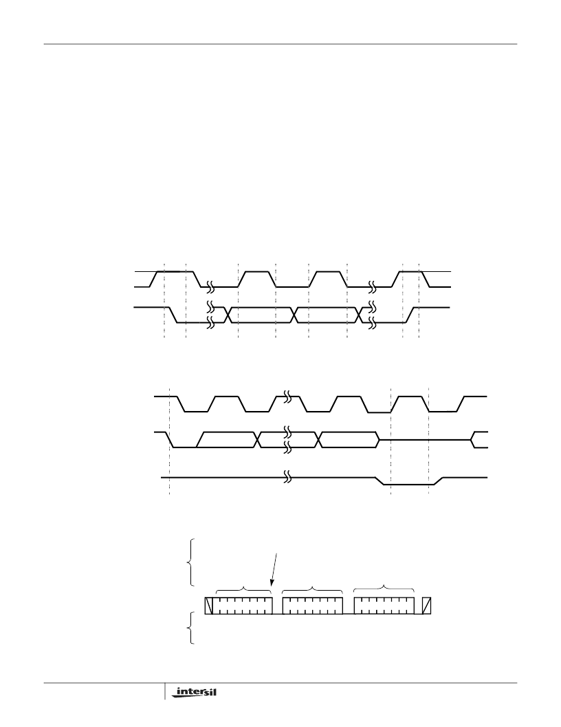
Protocol Conventions
Data states on the SDA line can change only during SCL
LOW periods. SDA state changes during SCL HIGH are
reserved for indicating START and STOP conditions (See
Figure 14). On power up of the ISL1219, the SDA pin is in
the input mode.
All I
2
C interface operations must begin with a START
condition, which is a HIGH to LOW transition of SDA while
SCL is HIGH. The ISL1219 continuously monitors the SDA
and SCL lines for the START condition and does not
respond to any command until this condition is met (See
Figure 14). A START condition is ignored during the
power-up sequence.
All I
2
C interface operations must be terminated by a STOP
condition, which is a LOW to HIGH transition of SDA while
SCL is HIGH (See Figure 14). A STOP condition at the end
of a read operation or at the end of a write operation to
memory only places the device in its standby mode.
An acknowledge (ACK) is a software convention used to
indicate a successful data transfer. The transmitting device,
either master or slave, releases the SDA bus after
transmitting eight bits. During the ninth clock cycle, the
receiver pulls the SDA line LOW to acknowledge the
reception of the eight bits of data (See Figure 15).
The ISL1219 responds with an ACK after recognition of a
START condition followed by a valid Identification Byte, and
once again after successful receipt of an Address Byte. The
ISL1219 also responds with an ACK after receiving a Data
Byte of a write operation. The master must respond with an
ACK after receiving a Data Byte of a read operation.
FIGURE 14. VALID DATA CHANGES, START, AND STOP CONDITIONS
FIGURE 15. ACKNOWLEDGE RESPONSE FROM RECEIVER
FIGURE 16. BYTE WRITE SEQUENCE
SDA
SCL
START
DATA
STABLE
DATA
CHANGE
STOP
DATA
STABLE
SDA OUTPUT FROM
TRANSMITTER
SDA OUTPUT FROM
RECEIVER
8
1
9
START
ACK
SCL FROM
MASTER
HIGH IMPEDANCE
HIGH IMPEDANCE
S
T
A
R
T
S
T
O
P
IDENTIFICATION
BYTE
DATA
BYTE
A
C
K
SIGNALS FROM
THE MASTER
SIGNALS FROM
THE ISL1219
A
C
K
1
0
0
1
1
A
C
K
WRITE
SIGNAL AT SDA
0 0 0 0
1 1 1
ADDRESS
BYTE
ISL1219
相关PDF资料 |
PDF描述 |
|---|---|
| ISL1220 | Low Power RTC with 8 Bytes of Battery Backed SRAM and Separate FOUT(具有电池供电的8位SRAM和独立输出的低功率RTC) |
| ISL1221 | Low Power RTC with Battery Backed SRAM and Event Detection(具有电池供电的SRAM和事件检测功能的低功率RTC) |
| ISL21009 | High Voltage Input Precision, Low Noise FGA Voltage References(高电压输入精度,低噪声FGA电压基准) |
| ISL21400 | Programmable Temperature Slope Voltage Reference(可编程温度斜率电压基准) |
| ISL22316 | Low Noise, Low Power I2C Bus, 128 Taps(低噪声,低功率,I2C总线, 128抽头电位器) |
相关代理商/技术参数 |
参数描述 |
|---|---|
| ISL1219IUZ | 功能描述:实时时钟 REAL TIME CLKRTC IN RoHS:否 制造商:Microchip Technology 功能:Clock, Calendar. Alarm RTC 总线接口:I2C 日期格式:DW:DM:M:Y 时间格式:HH:MM:SS RTC 存储容量:64 B 电源电压-最大:5.5 V 电源电压-最小:1.8 V 最大工作温度:+ 85 C 最小工作温度: 安装风格:Through Hole 封装 / 箱体:PDIP-8 封装:Tube |
| ISL1219IUZ-T | 功能描述:实时时钟 REAL TIME CLKRTC IN RoHS:否 制造商:Microchip Technology 功能:Clock, Calendar. Alarm RTC 总线接口:I2C 日期格式:DW:DM:M:Y 时间格式:HH:MM:SS RTC 存储容量:64 B 电源电压-最大:5.5 V 电源电压-最小:1.8 V 最大工作温度:+ 85 C 最小工作温度: 安装风格:Through Hole 封装 / 箱体:PDIP-8 封装:Tube |
| ISL1220 | 制造商:INTERSIL 制造商全称:Intersil Corporation 功能描述:I2C㈢ Real Time Clock/Calendar with Frequency Output |
| ISL1220IUZ | 功能描述:实时时钟 REAL TIME CLKRTC IN RoHS:否 制造商:Microchip Technology 功能:Clock, Calendar. Alarm RTC 总线接口:I2C 日期格式:DW:DM:M:Y 时间格式:HH:MM:SS RTC 存储容量:64 B 电源电压-最大:5.5 V 电源电压-最小:1.8 V 最大工作温度:+ 85 C 最小工作温度: 安装风格:Through Hole 封装 / 箱体:PDIP-8 封装:Tube |
| ISL1220IUZ-T | 功能描述:实时时钟 REAL TIME CLKRTC IN RoHS:否 制造商:Microchip Technology 功能:Clock, Calendar. Alarm RTC 总线接口:I2C 日期格式:DW:DM:M:Y 时间格式:HH:MM:SS RTC 存储容量:64 B 电源电压-最大:5.5 V 电源电压-最小:1.8 V 最大工作温度:+ 85 C 最小工作温度: 安装风格:Through Hole 封装 / 箱体:PDIP-8 封装:Tube |
发布紧急采购,3分钟左右您将得到回复。