参数资料
| 型号: | ISL55211IRTZ-T7A |
| 厂商: | Intersil |
| 文件页数: | 3/20页 |
| 文件大小: | 0K |
| 描述: | IC OPAMP DIFF LOW NOISE 16TQFN |
| 产品培训模块: | Solutions for Test and Measurement Equipment |
| 标准包装: | 1 |
| 放大器类型: | 差分 |
| 电路数: | 1 |
| 输出类型: | 差分 |
| 转换速率: | 5600 V/µs |
| -3db带宽: | 1.6GHz |
| 电流 - 输入偏压: | 50µA |
| 电压 - 输入偏移: | 100µV |
| 电流 - 电源: | 35mA |
| 电流 - 输出 / 通道: | 45mA |
| 电压 - 电源,单路/双路(±): | 3 V ~ 4.2 V |
| 工作温度: | -40°C ~ 85°C |
| 安装类型: | 表面贴装 |
| 封装/外壳: | 16-WFQFN 裸露焊盘 |
| 供应商设备封装: | 16-TQFN(3x3) |
| 包装: | 标准包装 |
| 其它名称: | ISL55211IRTZ-T7ADKR |
ISL55211
11
FN7868.0
June 21, 2011
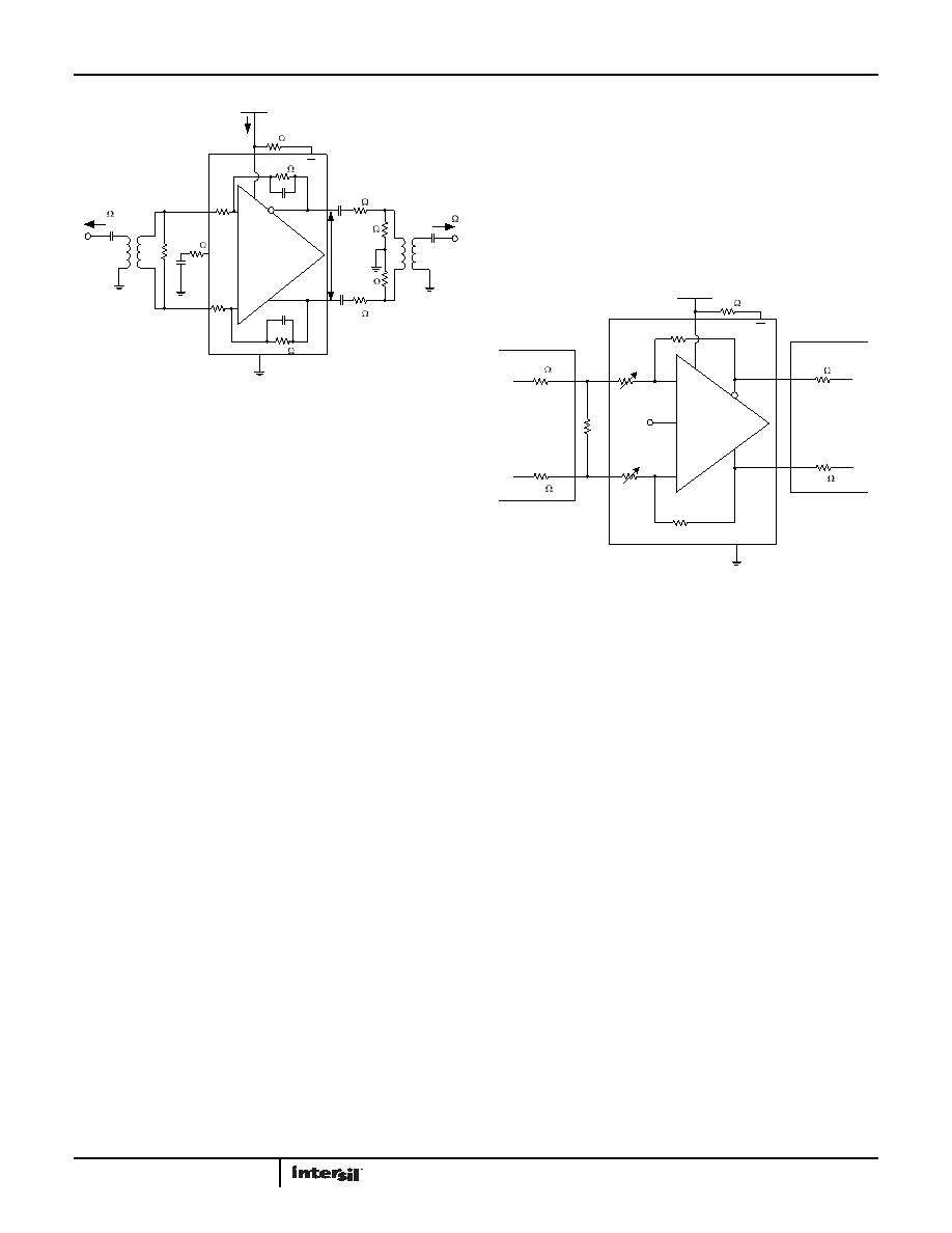
Working with a transformer coupled input as shown in Figure 29,
or with two DC blocking caps from a differential source, means
the output common mode voltage set by either the default
internal VCM setting, or a voltage applied to the VCM control pin,
will also appear as the input common mode voltage. This
provides a very easy way to control the ISL55211 I/O common
mode operating voltages for an AC-coupled signal path. The
internal common mode loop holds the output pins to VCM and,
since there is no DC path for an ICM current back towards the
common mode voltage. It is useful, for this reason, to leave any
input transformer secondary centertap unconnected. The
internally set VCM voltage is referenced from the negative supply
pin. With a single 3.3V supply, it is very close to 1.2V but will
change with total supply voltage across the device as shown in
Figure 27.
Most of the characterization curves starting with Figure 29 then
get different gains by changing the connections to the two pairs
of input RG connections, as shown on the pin configuration
drawing on page 2. Two input turns ratios are intended for Test
Circuit 1; either a 1:1.4 turns ratio (ohms ratio of 2) or a 1:2 turns
ratio (ohm ratio of 4). The specific transformers shown in
Figure 29 are representative of broadband RF transformers but
alternate devices and manufacturers of these turns ratio devices
are certainly applicable. The output side of this test circuit
presents a differential 200 load while converting the
differential to single-ended through a resistive attenuator and a
1:1 transformer. This inserts approximately a 17dB insertion loss
that is removed to report the characteristic curves. For load tests
below the 200 shown in Figure 29, a simple added shunt
resistor is placed across the output pins. For loads > 200, the
series and shunt load R's are adjusted to show that total load
(including the 50 measurement load reflected through the 1:1
output measurement port transformer) and provide an apparent
50 differential source to that transformer. This output side
transformer is for measurement purposes only and is not
necessary for final applications circuits. There are output
interface designs that do benefit from a transformer as part of
the signal path as shown in Figure 1. In that case, the 1:1:4
output side transformer becomes part of a filter design and
recovers the filter insertion loss from the amplifier output pins to
the ADC inputs.
Where just the amplifier is tested, a 4-port network analyzer is
used and the very simple test circuit of Figure 30 is
implemented. This is used to measure the differential S21 curves
vs gain of Figure 17 and as a simulation circuit for the differential
output impedance vs gain of Figure 18. Changing the gain is a
simple matter of adjusting the connections to the four input RG
connections resistors, as shown in Table 1. This circuit depends
on the two AC-coupled source 50
Ω of the 4 port network analyzer
and presents an AC-coupled differential 100
Ω load to the
amplifier as the input impedance of the remaining two ports of
the network analyzer.
Using this measurement allows the small single bandwidth of
just the ISL55211 to be exposed. Many of the other
measurements are using I/O transformers that are limiting the
apparent bandwidth to a reduced level. Figure 17 shows the 3
normalized differential S21 curves for the possible internal gains
of 9dB, 14dB and 15dB. The small signal bandwidth is remaining
nearly constant at 1.4GHz due to the internal capacitive
feedback network.
The closed loop differential output impedance of Figure 18 is
simulated using Figure 30 in ADS. This shows a relatively low
output impedance (< 1 through 100MHz) constant with signal
gain setting. Typical FDA outputs show a closed loop output
impedance that increases with signal gain setting. The ISL55211
holds a more constant response due to internal design elements
unique to this device.
Common mode output measurements are made using the circuit
in Figure 31. Here, the outputs are summed together through two
100 resistors (still a 200 differential load) to a center point
where the average, or common mode, output voltage may be
sensed. This is coupled through a 1F DC blocking capacitor and
measured using 50 test equipment. The common mode source
impedance for this circuit is the parallel combination of the
2-100 elements, or 50. Figure 19 uses this circuit to measure
the small and large signal response from the VCM control pin to
the output common mode. This pin includes an internal 50pF
capacitor on the default bias network (to filter supply noise when
there is no connection to this pin), which bandlimits the response
to approximately 30MHz. This is far lower than the actual
bandwidth of the common mode loop. Figure 20 uses this output
FIGURE 29. TEST CIRCUIT 1
50
1F
1:1.4
1F
85
ISL55211
+3.3V
+
-
Vi
35
ADT2-
1T
or
ADT4-
1Wt
0.1F
VCM
500
35mA
115mW
1:1
ADT1-
1WT
50
1F Vm
VO
RG
PD
0.2pF
RT
200
85
10k
FIGURE 30. TEST CIRCUIT 2 4-PORT S-PARAMETER
MEASUREMENTS
ISL55211
+3.3V
+
-
50
VCM
RF
50
1/2 of a 4-port
S-parameter
1/2 of a 4-port
S-parameter
10k
PD
RG
RT
50
相关PDF资料 |
PDF描述 |
|---|---|
| K10 12" X 12" | THERMAL PAD 12"X12" .006" K10 |
| K4-06 | THERMAL PAD 0.006" K4 |
| K6-0.006-AC-43 | THERMAL PAD TO-220 .006" K4 |
| KA324D | IC OPAMP QUAD HIGH GAIN 14-SOP |
| KA358STU | IC OPAMP DUAL HI GAIN 9-SIP |
相关代理商/技术参数 |
参数描述 |
|---|---|
| ISL55290 | 制造商:INTERSIL 制造商全称:Intersil Corporation 功能描述:Single and Dual Ultra-Low Noise, Ultra-Low Distortion, Low Power Op Amp |
| ISL55290EVAL1Z | 制造商:Intersil Corporation 功能描述:ISL55290 EVALUATION BOARD 1 - ROHS COMPLIANT - MSOP - Bulk |
| ISL55290IUZ | 功能描述:IC OPAMP LP DUAL ULT LN 10-MSOP RoHS:是 类别:集成电路 (IC) >> Linear - Amplifiers - Instrumentation 系列:- 标准包装:1 系列:- 放大器类型:通用 电路数:4 输出类型:满摆幅 转换速率:0.6 V/µs 增益带宽积:1MHz -3db带宽:- 电流 - 输入偏压:2pA 电压 - 输入偏移:1000µV 电流 - 电源:85µA 电流 - 输出 / 通道:20mA 电压 - 电源,单路/双路(±):1.8 V ~ 6 V 工作温度:-40°C ~ 125°C 安装类型:表面贴装 封装/外壳:14-SOIC(0.154",3.90mm 宽) 供应商设备封装:14-SOICN 包装:剪切带 (CT) 产品目录页面:680 (CN2011-ZH PDF) 其它名称:MCP6L04T-E/SLCT |
| ISL55290IUZ-T13 | 功能描述:IC OPAMP LP DUAL ULT LN 10-MSOP RoHS:是 类别:集成电路 (IC) >> Linear - Amplifiers - Instrumentation 系列:- 标准包装:1 系列:- 放大器类型:通用 电路数:4 输出类型:满摆幅 转换速率:0.6 V/µs 增益带宽积:1MHz -3db带宽:- 电流 - 输入偏压:2pA 电压 - 输入偏移:1000µV 电流 - 电源:85µA 电流 - 输出 / 通道:20mA 电压 - 电源,单路/双路(±):1.8 V ~ 6 V 工作温度:-40°C ~ 125°C 安装类型:表面贴装 封装/外壳:14-SOIC(0.154",3.90mm 宽) 供应商设备封装:14-SOICN 包装:剪切带 (CT) 产品目录页面:680 (CN2011-ZH PDF) 其它名称:MCP6L04T-E/SLCT |
| ISL55291 | 制造商:INTERSIL 制造商全称:Intersil Corporation 功能描述:Single and Dual Ultra-Low Noise, Ultra-Low Distortion, Rail-to-Rail, Low Power Op Amp |
发布紧急采购,3分钟左右您将得到回复。