参数资料
| 型号: | ISL55211IRTZ-T7A |
| 厂商: | Intersil |
| 文件页数: | 4/20页 |
| 文件大小: | 0K |
| 描述: | IC OPAMP DIFF LOW NOISE 16TQFN |
| 产品培训模块: | Solutions for Test and Measurement Equipment |
| 标准包装: | 1 |
| 放大器类型: | 差分 |
| 电路数: | 1 |
| 输出类型: | 差分 |
| 转换速率: | 5600 V/µs |
| -3db带宽: | 1.6GHz |
| 电流 - 输入偏压: | 50µA |
| 电压 - 输入偏移: | 100µV |
| 电流 - 电源: | 35mA |
| 电流 - 输出 / 通道: | 45mA |
| 电压 - 电源,单路/双路(±): | 3 V ~ 4.2 V |
| 工作温度: | -40°C ~ 85°C |
| 安装类型: | 表面贴装 |
| 封装/外壳: | 16-WFQFN 裸露焊盘 |
| 供应商设备封装: | 16-TQFN(3x3) |
| 包装: | 标准包装 |
| 其它名称: | ISL55211IRTZ-T7ADKR |
ISL55211
12
FN7868.0
June 21, 2011
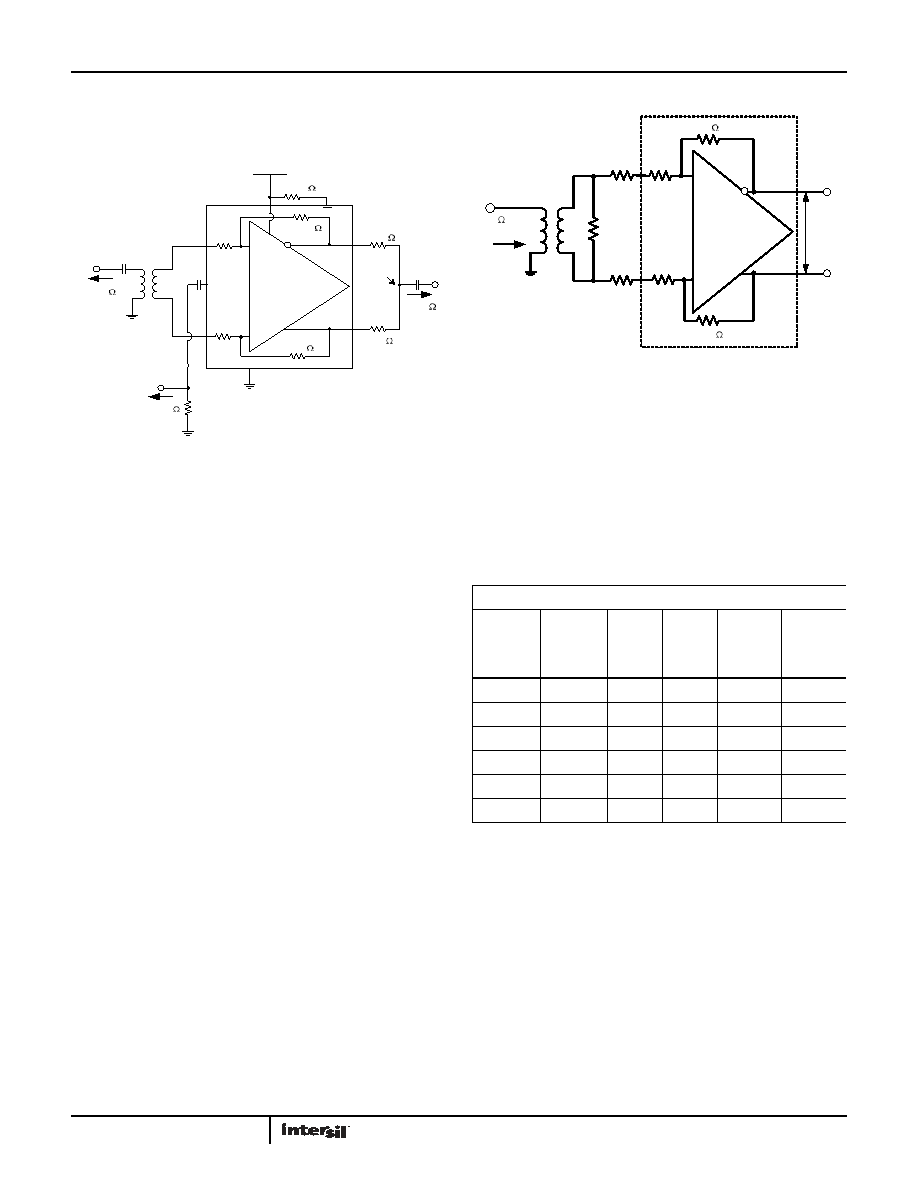
CM measurement circuit with a large signal (2VP-P) differential
output voltage (generated through the Vi path of Figure 31) to
measure the differential to common mode conversion - often
called the "Output Balance Error" for an FDA.
Single Supply, Input Transformer Coupled,
Design Considerations
The characterization circuit of Figure 29 shows one possible
input stage interface that offers several advantages. Where AC
coupling is adequate, the circuit of Figure 29 simplifies the input
common mode voltage control. If the source coming into this
stage is single-ended, the input transformer provides a zero
power conversion to differential. The two gain resistors (RG in
Figure 29) provide both a portion of the input termination
impedance and the gain element for the amplifier. For 50
systems, these RG resistors are too high with the turns ratios
shown in Figure 29 to provide the full match and an external RT
resistor is required. This RT element goes away at the highest
gain setting using a 1:2 input turns ratio transformer.
It is also possible to adapt this circuit to other input characteristic
while Table 2 shows the necessary external R values and
resulting gains.
Here, the sum of the two internal RG resistors at the higher two
gain settings is too low to retain a match for the 1:2 input step up
case. There, a pair of external series resistors are added to get
the total differential input impedance up to 300 on the
secondary side of the transformer and the RT element goes to
infinity. These two conditions are not particularly useful but
Figure 32 shows how to implement the full range of internal
conditions with the two turns ratios considered in Table 2.
Figure 32 also shows a pair of alternate input transformer types
from Pulse Engineering particularly suitable to the 75 case.
This input interface also simplifies the input common mode
control. The VCM pin controls the output common mode voltage.
In most DC-coupled FDA applications, the input common mode
voltage is determined by both this output common mode and the
source signal. In a configuration like Figure 29, there is no path
for a common mode current to flow from output to input, so the
input common mode voltage equals the output. A similar effect
could be achieved with just two blocking caps on the two RG
resistors. A DC-coupled, single to differential, configuration will
also have a common mode input that is moving with the input
signal. Converting to just a differential signal at the amplifier, as
in Figure 29, removes any input signal related artifacts from the
input common mode making the ISL55211 behave as a
differential only VFA amplifier. There is only a very small
differential error signal at the inputs set by the loop gain, as in a
FIGURE 31. TEST CIRCUIT #3 COMMON MODE AC OUTPUT
MEASUREMENTS
50
1F
1:1.4
ISL55211
+3.3V
+
-
RG
VCM
500
100
ADT2-1T
1F
Vi
10k
PD
50
Output
VCM
50
VCM Input
1F
TABLE 2. EXTERNAL RESISTORS FOR A 75
Ω INPUT
IMPEDANCE DESIGN
ISL55211 INTENDED TRANSFORMER + INTERNAL GAIN SETTINGS
INPUT
XFMR
TURNS
RATIO
INTERNAL
RG VALUE
(
Ω)
GAIN
(V/V)
VO/VI
GAIN
(dB)
VO/VI
EXTERNAL
RT VALUE
(
Ω)
EXTERNAL
RS VALUE
(
Ω)
1:1.4
250
2.8
9
214
0
1:1.4
125
5.6
15
375
0
1:1.4
100
7
17
600
0
1:2
250
4
12
750
0
1:2
125
6.7
16.5
Open
25
1:2
100
6.7
16.5
Open
50
FIGURE 32. 75
Ω IMPEDANCE IMPLEMENTATIONS
+
-
500
RG
1:n
75 INPUT
ISL55211
Vi
VO
RT
1:1.4 -> CX2045NL
1:2 -> CX2032
RS
相关PDF资料 |
PDF描述 |
|---|---|
| K10 12" X 12" | THERMAL PAD 12"X12" .006" K10 |
| K4-06 | THERMAL PAD 0.006" K4 |
| K6-0.006-AC-43 | THERMAL PAD TO-220 .006" K4 |
| KA324D | IC OPAMP QUAD HIGH GAIN 14-SOP |
| KA358STU | IC OPAMP DUAL HI GAIN 9-SIP |
相关代理商/技术参数 |
参数描述 |
|---|---|
| ISL55290 | 制造商:INTERSIL 制造商全称:Intersil Corporation 功能描述:Single and Dual Ultra-Low Noise, Ultra-Low Distortion, Low Power Op Amp |
| ISL55290EVAL1Z | 制造商:Intersil Corporation 功能描述:ISL55290 EVALUATION BOARD 1 - ROHS COMPLIANT - MSOP - Bulk |
| ISL55290IUZ | 功能描述:IC OPAMP LP DUAL ULT LN 10-MSOP RoHS:是 类别:集成电路 (IC) >> Linear - Amplifiers - Instrumentation 系列:- 标准包装:1 系列:- 放大器类型:通用 电路数:4 输出类型:满摆幅 转换速率:0.6 V/µs 增益带宽积:1MHz -3db带宽:- 电流 - 输入偏压:2pA 电压 - 输入偏移:1000µV 电流 - 电源:85µA 电流 - 输出 / 通道:20mA 电压 - 电源,单路/双路(±):1.8 V ~ 6 V 工作温度:-40°C ~ 125°C 安装类型:表面贴装 封装/外壳:14-SOIC(0.154",3.90mm 宽) 供应商设备封装:14-SOICN 包装:剪切带 (CT) 产品目录页面:680 (CN2011-ZH PDF) 其它名称:MCP6L04T-E/SLCT |
| ISL55290IUZ-T13 | 功能描述:IC OPAMP LP DUAL ULT LN 10-MSOP RoHS:是 类别:集成电路 (IC) >> Linear - Amplifiers - Instrumentation 系列:- 标准包装:1 系列:- 放大器类型:通用 电路数:4 输出类型:满摆幅 转换速率:0.6 V/µs 增益带宽积:1MHz -3db带宽:- 电流 - 输入偏压:2pA 电压 - 输入偏移:1000µV 电流 - 电源:85µA 电流 - 输出 / 通道:20mA 电压 - 电源,单路/双路(±):1.8 V ~ 6 V 工作温度:-40°C ~ 125°C 安装类型:表面贴装 封装/外壳:14-SOIC(0.154",3.90mm 宽) 供应商设备封装:14-SOICN 包装:剪切带 (CT) 产品目录页面:680 (CN2011-ZH PDF) 其它名称:MCP6L04T-E/SLCT |
| ISL55291 | 制造商:INTERSIL 制造商全称:Intersil Corporation 功能描述:Single and Dual Ultra-Low Noise, Ultra-Low Distortion, Rail-to-Rail, Low Power Op Amp |
发布紧急采购,3分钟左右您将得到回复。