参数资料
| 型号: | ISL55211IRTZ-T7A |
| 厂商: | Intersil |
| 文件页数: | 6/20页 |
| 文件大小: | 0K |
| 描述: | IC OPAMP DIFF LOW NOISE 16TQFN |
| 产品培训模块: | Solutions for Test and Measurement Equipment |
| 标准包装: | 1 |
| 放大器类型: | 差分 |
| 电路数: | 1 |
| 输出类型: | 差分 |
| 转换速率: | 5600 V/µs |
| -3db带宽: | 1.6GHz |
| 电流 - 输入偏压: | 50µA |
| 电压 - 输入偏移: | 100µV |
| 电流 - 电源: | 35mA |
| 电流 - 输出 / 通道: | 45mA |
| 电压 - 电源,单路/双路(±): | 3 V ~ 4.2 V |
| 工作温度: | -40°C ~ 85°C |
| 安装类型: | 表面贴装 |
| 封装/外壳: | 16-WFQFN 裸露焊盘 |
| 供应商设备封装: | 16-TQFN(3x3) |
| 包装: | 标准包装 |
| 其它名称: | ISL55211IRTZ-T7ADKR |
ISL55211
14
FN7868.0
June 21, 2011
The ISL55211 includes a power shutdown feature that can be used
to reduce system power dissipation when signal path operation is
not required. This pin (Pd) is referenced to -Vs and must be asserted
low to activate the shutdown feature. When not used, a 10k
external resistor to +Vs should be used to assert a high level at this
pin. Digital control on this pin can be either an open collector output
(using that 10k pull-up) or a CMOS logic line running off the same
+Vs as the amplifier. For split supply operation, the Pd pins must be
pulled to below -Vs + 0.54V to disable.
Since the ISL55211 operates as a differential inverting op amp,
there is only modest signal path isolation when disabled, as shown
in Figure 24. The inputs include 2 pairs of back to back low
capacitance diodes intended to protect any subsequent devices
from large input signals during shutdown. Those diodes limit the
maximum overdrive voltage across the input to approximately 1.0V
in each polarity. The internal RG resistors of Test Circuit 1 limit the
current into those diodes under this condition.
The supply current in shutdown does not reduce to zero as internal
circuitry is still active to hold the output common mode voltage at
the VCM voltage even during shutdown. This is intended to hold the
ISL55211 outputs near the desired common mode output level
during shutdown. This improves the turn on characteristic and keeps
those output voltages in a safe range for downstream circuitry.
The very low internal power dissipation of the ISL55211, along with
the excellent thermal conductivity of the TQFN package when the
exposed metal pad is tied to a conductive plate, reduces the TJ rise
above ambient to very modest levels. Assuming a nominal 115mW
dissipation and using the 63°C/W measured thermal impedance
from Junction to ambient, gives a rise of only 0.115*63 = 7.2°C.
Operation at elevated ambient temperatures is easily supported
given this very low internal rise to junction.
The maximum internal junction temperatures would occur at
maximum supply voltage, +85°C maximum ambient operating,
and where the TQFN exposed pad is not tied to a conductive layer.
Where the TQFN must be mounted with an insulating layer to the
exposed metal plate, such as in a split supply application, device
measurements show an increased thermal impedance junction to
ambient of +120°C/W. Using this, and a maximum quiescent
internal power on 4.5V absolute maximum, which shows 45mA for
+85°C maximum operating ambient from Figure 27, we get
4.5V*45mA*+120°C/W = +24°C rise above +85°C or
approximately +109°C operating TJ maximum - still well below the
specified Absolute Maximum operating junction temperature of
+135°C.
Noise Analysis
The decompensated voltage feedback design of the ISL55211
provides very low input voltage and current noise. Based on the
ISL55210, these internal noise terms are 0.85nV/√Hz differential
voltage noise and a 5pA/√Hz current noise term on each side. Since
the ISL55211 is an internally fixed gain version, these internal noise
terms will produce only a few set of output noise values. Figure 34
shows the analysis model for just the ISL55211 with no input
transformer while Table 3 shows the resulting output and input
referred differential spot noise voltages using Equation 1.
With equal feedback and gain resistors, the total output noise
expression becomes very simple. This is shown as Equation 1.
The NG term in this equation is the Noise Gain = 1 + RF/RG. The
noise terms. Table 3 evaluates this expression for the 3 possible
internal gains with a fixed 500 internal feedback. nV/√HZ
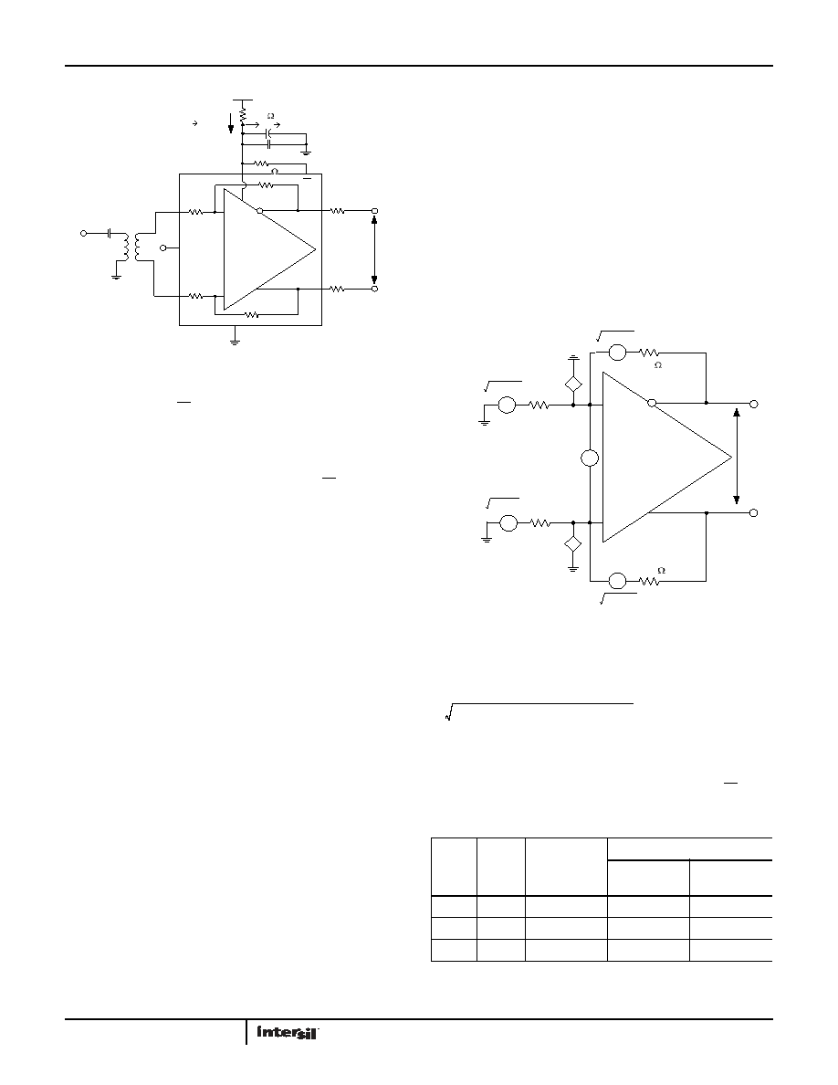
FIGURE 33. OPERATING FROM A SINGLE +5V SUPPLY
CIN 1:n
ISL55211
+5V ±5%
+
-
Vi
VCM
VO
RF
RG
10k
PD
RO
24.3
35
55mA
3.4
4.4V
10nF
2.2F
+
TABLE 3. OUTPUT AND INPUT SPOT NOISE FROM EQUATION 1 FOR
THE 3 GAINS OF THE ISL55211
RG
(
Ω)
GAIN
V/V
NOISE GAIN
V/V
INPUT REFERRED
EO
nV/√Hz
ENI
nV/√Hz
250
2
3
8.19
4.09
125
4
5
10.51
2.63
100
5
6
11.60
2.32
FIGURE 34. AMPLIFIER ONLY NOISE MODEL
ISL55211
+
-
eO
RF
RG
*
iN
4kTRG
*
iN
*
4kTRF
*
en
500
4kTRG
(EQ. 1)
e0 eNNG
()2 2iNRF
()2 24kTRFNG
()
++
相关PDF资料 |
PDF描述 |
|---|---|
| K10 12" X 12" | THERMAL PAD 12"X12" .006" K10 |
| K4-06 | THERMAL PAD 0.006" K4 |
| K6-0.006-AC-43 | THERMAL PAD TO-220 .006" K4 |
| KA324D | IC OPAMP QUAD HIGH GAIN 14-SOP |
| KA358STU | IC OPAMP DUAL HI GAIN 9-SIP |
相关代理商/技术参数 |
参数描述 |
|---|---|
| ISL55290 | 制造商:INTERSIL 制造商全称:Intersil Corporation 功能描述:Single and Dual Ultra-Low Noise, Ultra-Low Distortion, Low Power Op Amp |
| ISL55290EVAL1Z | 制造商:Intersil Corporation 功能描述:ISL55290 EVALUATION BOARD 1 - ROHS COMPLIANT - MSOP - Bulk |
| ISL55290IUZ | 功能描述:IC OPAMP LP DUAL ULT LN 10-MSOP RoHS:是 类别:集成电路 (IC) >> Linear - Amplifiers - Instrumentation 系列:- 标准包装:1 系列:- 放大器类型:通用 电路数:4 输出类型:满摆幅 转换速率:0.6 V/µs 增益带宽积:1MHz -3db带宽:- 电流 - 输入偏压:2pA 电压 - 输入偏移:1000µV 电流 - 电源:85µA 电流 - 输出 / 通道:20mA 电压 - 电源,单路/双路(±):1.8 V ~ 6 V 工作温度:-40°C ~ 125°C 安装类型:表面贴装 封装/外壳:14-SOIC(0.154",3.90mm 宽) 供应商设备封装:14-SOICN 包装:剪切带 (CT) 产品目录页面:680 (CN2011-ZH PDF) 其它名称:MCP6L04T-E/SLCT |
| ISL55290IUZ-T13 | 功能描述:IC OPAMP LP DUAL ULT LN 10-MSOP RoHS:是 类别:集成电路 (IC) >> Linear - Amplifiers - Instrumentation 系列:- 标准包装:1 系列:- 放大器类型:通用 电路数:4 输出类型:满摆幅 转换速率:0.6 V/µs 增益带宽积:1MHz -3db带宽:- 电流 - 输入偏压:2pA 电压 - 输入偏移:1000µV 电流 - 电源:85µA 电流 - 输出 / 通道:20mA 电压 - 电源,单路/双路(±):1.8 V ~ 6 V 工作温度:-40°C ~ 125°C 安装类型:表面贴装 封装/外壳:14-SOIC(0.154",3.90mm 宽) 供应商设备封装:14-SOICN 包装:剪切带 (CT) 产品目录页面:680 (CN2011-ZH PDF) 其它名称:MCP6L04T-E/SLCT |
| ISL55291 | 制造商:INTERSIL 制造商全称:Intersil Corporation 功能描述:Single and Dual Ultra-Low Noise, Ultra-Low Distortion, Rail-to-Rail, Low Power Op Amp |
发布紧急采购,3分钟左右您将得到回复。