参数资料
| 型号: | ISL55211IRTZ-T7A |
| 厂商: | Intersil |
| 文件页数: | 7/20页 |
| 文件大小: | 0K |
| 描述: | IC OPAMP DIFF LOW NOISE 16TQFN |
| 产品培训模块: | Solutions for Test and Measurement Equipment |
| 标准包装: | 1 |
| 放大器类型: | 差分 |
| 电路数: | 1 |
| 输出类型: | 差分 |
| 转换速率: | 5600 V/µs |
| -3db带宽: | 1.6GHz |
| 电流 - 输入偏压: | 50µA |
| 电压 - 输入偏移: | 100µV |
| 电流 - 电源: | 35mA |
| 电流 - 输出 / 通道: | 45mA |
| 电压 - 电源,单路/双路(±): | 3 V ~ 4.2 V |
| 工作温度: | -40°C ~ 85°C |
| 安装类型: | 表面贴装 |
| 封装/外壳: | 16-WFQFN 裸露焊盘 |
| 供应商设备封装: | 16-TQFN(3x3) |
| 包装: | 标准包装 |
| 其它名称: | ISL55211IRTZ-T7ADKR |
ISL55211
15
FN7868.0
June 21, 2011
Adding an input transformer can improve the input referred noise
by adding a noiseless voltage gain. Starting from Test Circuit 1 of
Figure 29, and assuming the source shows a matched
broadband source RS that will be matched by the input referred
parallel combination of 2*RG||RT, a noise gain analysis circuit
can be developed as shown in Figure 35.
Stepping through the 3 gain settings with two input transformers
will allow the noise gain to be calculated for the circuit of
output differential noise (since RF is fixed at 500). Doing this
gives Table 4.
The signal gain is taken from the input of the transformer for this
analysis and shows the total input referred noise going below
0.9nV at the highest gain setting here. While this analysis is
including the approximate 0.9nV noise of a 50 source R, that
noise is assumed to be divided down by 2 to the input of the
transformer, which explains the total input referred noise
showing up as less than just a 50 resistor. The total output
differential noise goes below 9nV/√Hz at the higher gains
settings using this input transformer technique. For even lower
noise, consider the ISL55210 where the input RT element is
generally not required. In that case, simply setting RG to the
desired input Z and adjusting RF to the desired gain will give an
output noise that is slightly lower than shown previously for the
same input transformer due to the removal of the RT element.
Driving Cap and Filter Loads
Most applications will drive a resistive or filter load. The
ISL55211 is robust to direct capacitive load on the outputs up to
approximately 10pF. For frequency response flatness, it is best to
avoid any output pin capacitance as much as possible - as the
capacitance increases, the high frequency portion of the
ISL55211 (>1GHz) response will start to show considerable
peaking. No oscillations were observed up through 10pF load on
each output.
For AC-coupled applications, an output network that is a small
series resistor (10 to 50) into a blocking capacitor is preferred.
This series resistor will isolate parasitic capacitance to ground
from the internally closed loop output stage of the amplifier and
de-que the self resonance of the blocking capacitors. Once the
output stage sees this resistive element first, the remaining part
of a passive filter design can be done without fear of amplifier
instability.
Driving ADC's
Many of the intended applications for the ISL55211 are as a low
power, very high dynamic range, last stage interface to high
performance ADC's. The lowest power ADC's, such as the
ISLA214P50 shown on the front page, include an innovative
"Femto-Charge" internal architecture that eliminates op amps
from the ADC design and only passes signal charge from stage to
stage. This greatly reduces the required quiescent power for
these ADC's but then that signal charge has to be provided by the
external circuit at the two input pins. This appears on an ADC like
the ISLA112P50 as a clock rate dependent common mode input
current that must be supplied by the interface circuit. At
500MHz, this DC current is 1.3mA on each input for the 14-bit
ISLA214P50.
Most interfaces will also include an interstage noise power
bandlimiting filter between the amplifier and the ADC. This filter
needs to be designed considering the loading of the amplifier,
any VCM level shifting that needs to take place, the filter shape,
and this Icm issue into the ADC input pins. Here are 4 example
topologies suitable for different situations.
1. AC-coupled, broadband RLC interstage filter design. This
approach lets the amplifier operate at its desired output
common mode, then provides the ADC common mode
voltage and current through a bias path as part of the filters
designs last stage R values. The Vb is set to include the IR loss
from that voltage to the ADC inputs due to the ICM current.
TABLE 4. OUTPUT NOISE AND INPUT REFERRED EQUIVALENT NOISE FOR THE TRANSFORMER COUPLED INPUT
ISL55211 INTENDED TRANSFORMER + INTERNAL GAIN SETTINGS
NOISE GAIN
V/V
INPUT REFERRED
INPUT XFMR
TURNS RATIO
INTERNAL
RG VALUE (Ω)
GAIN (V/V)
VO/VI
GAIN (dB)
VO/VI
EXTERNAL
RT VALUE (Ω)
TOTAL GAIN
RESISTOR FOR
NG (
Ω)
EO
nV/√Hz
ENI
nV/√Hz
1:1.4
250
2.8
9
122
277.48
2.80
7.94
2.834811
1:1.4
125
5.6
15
162
155.92
4.21
9.62
1.718338
1:1.4
100
7
17
192
132.88
4.76
10.25
1.46452
1:2
250
4
12
333
312.48
2.60
7.68
1.920066
1:2
125
8
18
1020
208.61
3.40
8.67
1.083876
1:2
100
10
20
1008
200.00
3.50
8.79
0.879492
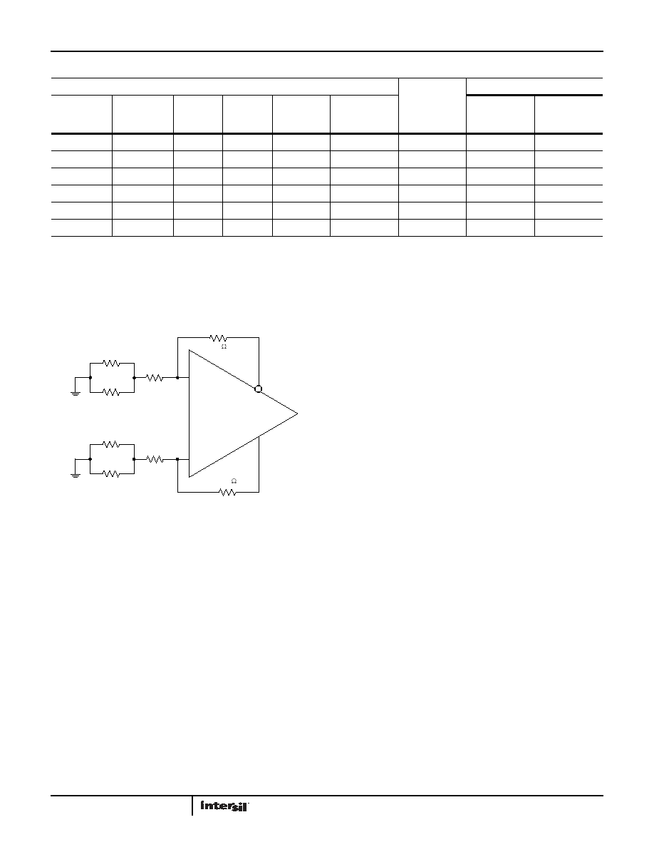
FIGURE 35. NOISE GAIN MODEL FOR THE TRANSFORMER
COUPLED INPUT CIRCUIT OF FIGURE 29
ISL55211
+
-
RF
RG
500
n2RS/2
RT/2
n2RS/2
RT/2
500
相关PDF资料 |
PDF描述 |
|---|---|
| K10 12" X 12" | THERMAL PAD 12"X12" .006" K10 |
| K4-06 | THERMAL PAD 0.006" K4 |
| K6-0.006-AC-43 | THERMAL PAD TO-220 .006" K4 |
| KA324D | IC OPAMP QUAD HIGH GAIN 14-SOP |
| KA358STU | IC OPAMP DUAL HI GAIN 9-SIP |
相关代理商/技术参数 |
参数描述 |
|---|---|
| ISL55290 | 制造商:INTERSIL 制造商全称:Intersil Corporation 功能描述:Single and Dual Ultra-Low Noise, Ultra-Low Distortion, Low Power Op Amp |
| ISL55290EVAL1Z | 制造商:Intersil Corporation 功能描述:ISL55290 EVALUATION BOARD 1 - ROHS COMPLIANT - MSOP - Bulk |
| ISL55290IUZ | 功能描述:IC OPAMP LP DUAL ULT LN 10-MSOP RoHS:是 类别:集成电路 (IC) >> Linear - Amplifiers - Instrumentation 系列:- 标准包装:1 系列:- 放大器类型:通用 电路数:4 输出类型:满摆幅 转换速率:0.6 V/µs 增益带宽积:1MHz -3db带宽:- 电流 - 输入偏压:2pA 电压 - 输入偏移:1000µV 电流 - 电源:85µA 电流 - 输出 / 通道:20mA 电压 - 电源,单路/双路(±):1.8 V ~ 6 V 工作温度:-40°C ~ 125°C 安装类型:表面贴装 封装/外壳:14-SOIC(0.154",3.90mm 宽) 供应商设备封装:14-SOICN 包装:剪切带 (CT) 产品目录页面:680 (CN2011-ZH PDF) 其它名称:MCP6L04T-E/SLCT |
| ISL55290IUZ-T13 | 功能描述:IC OPAMP LP DUAL ULT LN 10-MSOP RoHS:是 类别:集成电路 (IC) >> Linear - Amplifiers - Instrumentation 系列:- 标准包装:1 系列:- 放大器类型:通用 电路数:4 输出类型:满摆幅 转换速率:0.6 V/µs 增益带宽积:1MHz -3db带宽:- 电流 - 输入偏压:2pA 电压 - 输入偏移:1000µV 电流 - 电源:85µA 电流 - 输出 / 通道:20mA 电压 - 电源,单路/双路(±):1.8 V ~ 6 V 工作温度:-40°C ~ 125°C 安装类型:表面贴装 封装/外壳:14-SOIC(0.154",3.90mm 宽) 供应商设备封装:14-SOICN 包装:剪切带 (CT) 产品目录页面:680 (CN2011-ZH PDF) 其它名称:MCP6L04T-E/SLCT |
| ISL55291 | 制造商:INTERSIL 制造商全称:Intersil Corporation 功能描述:Single and Dual Ultra-Low Noise, Ultra-Low Distortion, Rail-to-Rail, Low Power Op Amp |
发布紧急采购,3分钟左右您将得到回复。