- 您现在的位置:买卖IC网 > PDF目录20330 > ISL6146AFUZ-T (Intersil)IC OR CTRLR N-CH 1CH 8MSOP PDF资料下载
参数资料
| 型号: | ISL6146AFUZ-T |
| 厂商: | Intersil |
| 文件页数: | 18/28页 |
| 文件大小: | 0K |
| 描述: | IC OR CTRLR N-CH 1CH 8MSOP |
| 标准包装: | 2,500 |
| 应用: | 电信/数据通信系统 |
| FET 型: | N 沟道 |
| 输出数: | 1 |
| 内部开关: | 无 |
| 延迟时间 - 关闭: | 65ns |
| 电源电压: | 1 V ~ 20 V |
| 工作温度: | -40°C ~ 125°C |
| 安装类型: | 表面贴装 |
| 封装/外壳: | 8-TSSOP,8-MSOP(0.118",3.00mm 宽) |
| 供应商设备封装: | 8-MSOP |
| 包装: | 带卷 (TR) |
第1页第2页第3页第4页第5页第6页第7页第8页第9页第10页第11页第12页第13页第14页第15页第16页第17页当前第18页第19页第20页第21页第22页第23页第24页第25页第26页第27页第28页
�� �
�
�ISL6146�
�Applications� Information�
�Power-Up� Considerations�
�BIAS� AND� V� IN� CONSTRAINTS�
�Upon� power-up� when� the� V� IN� supply� is� separate� from� the� BIAS�
�supply,� the� BIAS� voltage� must� be� greater� or� equal� to� the� V� IN�
�voltage� at� all� times.�
�When� using� a� single� supply� for� both� the� ISL6146� bias� and� the�
�OR-ing� supply,� the� V� IN� and� BIAS� pins� can� be� configured� with� a� low�
�value� resistor� between� the� two� pins� to� provide� some� isolation� and�
�decoupling� to� support� the� chip� bias� even� as� the� OR’d� supply�
�experiences� voltage� droops� and� surges.� Although� not� necessary�
�to� do� so,� it� is� a� best� design� practice� for� particularly� noisy�
�environments.�
�FET� TO� IC� LAYOUT� RECOMMENDATIONS�
�Connections� from� the� FET(s)� to� the� ISL6146� VIN� and� VOUT� pins�
�must� be� Kelvin� in� nature� and� as� close� to� the� FET� drain� and� source�
�PCB� pads� as� possible� to� eliminate� any� trace� resistance� errors�
�that� can� occur� with� high� currents.� This� connection� placement� is�
�most� critical� to� providing� the� most� accurate� voltage� sensing�
�particularly� when� the� back-to-back� FET� configuration� is� used.�
�Likewise,� connections� from� OVP,� UVLO� and� ADJ� are� also� critical� to�
�optimize� accuracy.�
�ADJUSTING� THE� HS� COMPARATOR� REVERSE� VOLTAGE�
�THRESHOLD�
�The� ISL6146� allows� adjustment� of� the� HS� Comparator� reverse�
�voltage� detection� threshold� (VR� Vth),� the� difference� in� V� OUT� -� V� IN� .�
�There� are� two� valid� ADJ� pin� configurations:�
�In� this� configuration,� it� may� be� tempting� to� use� the� enable� inputs�
�to� force� a� path� by� switching� between� the� two� as� opposed� to�
�having� both� paths� on,� and� having� the� higher� voltage� source�
�provide� current.� The� problem� with� that� is� the� timing� of� the� FETs�
�on� and� off,� so� that� excessive� V� OUT� voltage� droop� is� not� introduced�
�if� the� turn-off� happens� faster,� or� before� the� (or� a� slower)� turn-on�
�momentarily� leaves� the� load� with� an� inadequate� power�
�connection.�
�Typical� Applications� Circuits�
�There� are� four� basic� configurations� that� the� ISL6146� can� be�
�used� in:�
�1.� For� voltages� >3V� where� the� BIAS� and� V� IN� are� common�
�2.� For� a� very� low� OR-ing� voltage,� <3V� operation,� BIAS� >3V�
�3.� For� a� voltage� window� compliant� operation� and,�
�4.� For� a� signaled� operation� where� the� current� path� is� controlled�
�by� an� input� signal� or� minimum� voltage� condition.�
�Each� of� these� configurations� can� be� tailored� for� the� High� Speed�
�Comparator� (HS� COMP)� reverse� threshold� via� the� ADJ� input� being�
�connected� either� to� VOUT� or� to� GND� via� a� resistor� as� previously�
�explained.� Additionally,� the� voltage� window� is� adjustable� for� both�
�a� minimum� and� maximum� operating� voltage� via� the� UVLO� and�
�OVP� inputs� and� a� resistor� divider� also� explained� earlier.� Also,�
�soft-start� and� turn-on� and� turn-off� characteristics� can� be� tailored�
�to� suit.�
�The� three� evaluation� platforms� provided� demonstrate� the� four�
�basic� configurations� and� provide� for� the� additional� tailoring� of�
�the� various� performance� characteristics.�
�BIAS�
�1.� ADJ� connected� to� VOUT:� This� makes� the� HS� comparator�
�threshold� equal� to� the� intrinsic� error� in� the� HS� comparator�
�VOLTAGE�
�>3V�
�Q1�
�+�
�input.� This� is� the� default� condition� and� the� most� likely� used�
�configuration.�
�2.� A� single� resistor� is� connected� from� ADJ� pin� to� ground:�
�Making� the� HS� comparator� threshold� =� V� OUT� -� 4k/R� ADJ� .�
�So,� for� a� 100k� ?� R� EXT� ,� HS� Comparator� threshold� =� 40mV� below�
�VOUT� and� for� a� 5k� ?� R� EXT� HS� comparator� threshold� =� ~� 800mV�
�below� VOUT.�
�The� recommended� resistor� range� is� 5k� ?� to� 100k� ?� for� this�
�voltage� adjustment.�
�+�
�VERY� LOW�
�VOLTAGE�
�DC� -� DC�
�(1V-3V)�
�-�
�VIN�
�BIAS�
�EN�
�GATE�
�ISL6146A�
�GND�
�VOUT�
�ADJ�
�FLT�
�C�
�O�
�M�
�M�
�O�
�N�
�P�
�O�
�W�
�E�
�R�
�B�
�U�
�S�
�At� power-up,� the� HS� comparator� threshold� is� default� set� to� the�
�+�
�internal� device� error� first,� and� then� released� to� the� user�
�programmed� threshold� after� the� related� circuits� are� ready.� It�
�takes� ~20� μ� s� for� the� circuit� to� switch� from� the� default� setting� to�
�the� user� programmed� threshold� after� a� POR� startup.�
�+�
�Q2�
�C�
�O�
�M�
�M�
�O�
�N�
�The� current� out� of� the� ADJ� pin� with� a� resistor� to� GND� is� equal� to�
�0.4V/R� EXT.�
�BACK-TO-BACK� FET� CONFIGURATION�
�When� using� the� back-to-back� FET� configuration,� the� FET� choice�
�must� be� such� that� the� voltage� across� both� FETs� at� full� current�
�loading� be� less� than� the� minimum� forward� voltage� fault�
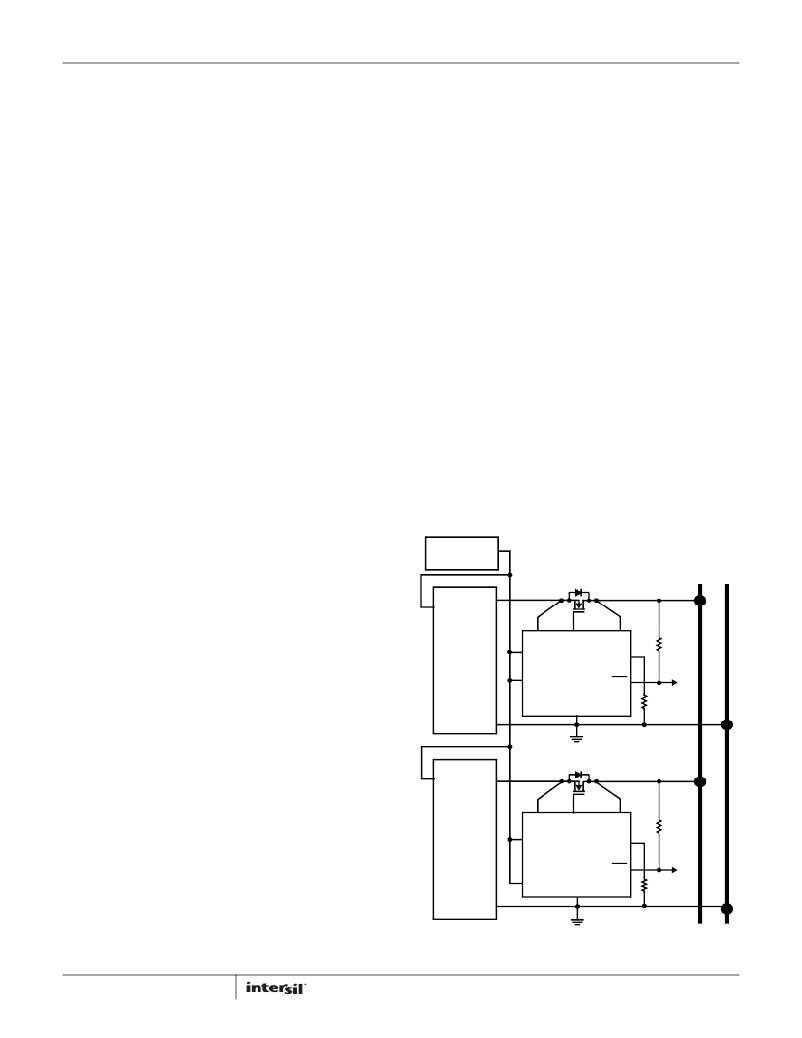
�VERY� LOW�
�VOLTAGE�
�DC� -� DC�
�(1V-3V)�
�-�
�VIN�
�BIAS�
�EN�
�GATE�
�ISL6146A�
�GND�
�VOUT�
�ADJ�
�FLT�
�P�
�O�
�W�
�E�
�R�
�B�
�U�
�S�
�threshold� of� 400mV� to� avoid� unintended� fault� notification.�
�FIGURE� 47.� LOW� VOLTAGE� APPLICATION� DIAGRAM�
�18�
�FN7667.4�
�April� 26,� 2013�
�相关PDF资料 |
PDF描述 |
|---|---|
| ISL6146CFRZ-TK | IC OR CONTROLLER |
| ISL6146CFRZ-T | IC OR CONTROLLER |
| ISL6146CFRZ | IC OR CONTROLLER |
| ISL6146BFRZ-TK | IC OR CONTROLLER |
| ISL6146BFRZ-T | IC INTERFACE |
相关代理商/技术参数 |
参数描述 |
|---|---|
| ISL6146AFUZ-T7A | 功能描述:热插拔功率分布 LWV ORING FET CNTRLR 8LD RoHS:否 制造商:Texas Instruments 产品:Controllers & Switches 电流限制: 电源电压-最大:7 V 电源电压-最小:- 0.3 V 工作温度范围: 功率耗散: 安装风格:SMD/SMT 封装 / 箱体:MSOP-8 封装:Tube |
| ISL6146AFUZ-TK | 功能描述:IC OR CTRLR N-CH 1CH 8MSOP RoHS:是 类别:集成电路 (IC) >> PMIC - O 圈控制器 系列:- 标准包装:1,000 系列:- 应用:电池备份,工业/汽车,大电流开关 FET 型:- 输出数:5 内部开关:是 延迟时间 - 开启:100ns 延迟时间 - 关闭:- 电源电压:3 V ~ 5.5 V 电流 - 电源:250µA 工作温度:0°C ~ 70°C 安装类型:表面贴装 封装/外壳:16-SOIC(0.154",3.90mm 宽) 供应商设备封装:16-SOIC N 包装:带卷 (TR) |
| ISL6146B | 制造商:INTERSIL 制造商全称:Intersil Corporation 功能描述:Low Voltage ORing FET Controller |
| ISL6146BEVAL1Z | 制造商:Intersil Corporation 功能描述:ISL6146B EVALUATION BOARD - 8 LEAD - MSOP - ROHS COMPLIANT - Bulk 制造商:Intersil Corporation 功能描述:BOARD EVAL FOR ISL6146 制造商:Intersil 功能描述:ISL98003CNZ-EVALZ EVAL BRD RHS COMPLIA |
| ISL6146BFRZ | 功能描述:IC INTERFACE RoHS:是 类别:集成电路 (IC) >> PMIC - O 圈控制器 系列:* 标准包装:1,000 系列:- 应用:电池备份,工业/汽车,大电流开关 FET 型:- 输出数:5 内部开关:是 延迟时间 - 开启:100ns 延迟时间 - 关闭:- 电源电压:3 V ~ 5.5 V 电流 - 电源:250µA 工作温度:0°C ~ 70°C 安装类型:表面贴装 封装/外壳:16-SOIC(0.154",3.90mm 宽) 供应商设备封装:16-SOIC N 包装:带卷 (TR) |
发布紧急采购,3分钟左右您将得到回复。