- 您现在的位置:买卖IC网 > PDF目录20330 > ISL6146AFUZ-T (Intersil)IC OR CTRLR N-CH 1CH 8MSOP PDF资料下载
参数资料
| 型号: | ISL6146AFUZ-T |
| 厂商: | Intersil |
| 文件页数: | 19/28页 |
| 文件大小: | 0K |
| 描述: | IC OR CTRLR N-CH 1CH 8MSOP |
| 标准包装: | 2,500 |
| 应用: | 电信/数据通信系统 |
| FET 型: | N 沟道 |
| 输出数: | 1 |
| 内部开关: | 无 |
| 延迟时间 - 关闭: | 65ns |
| 电源电压: | 1 V ~ 20 V |
| 工作温度: | -40°C ~ 125°C |
| 安装类型: | 表面贴装 |
| 封装/外壳: | 8-TSSOP,8-MSOP(0.118",3.00mm 宽) |
| 供应商设备封装: | 8-MSOP |
| 包装: | 带卷 (TR) |
第1页第2页第3页第4页第5页第6页第7页第8页第9页第10页第11页第12页第13页第14页第15页第16页第17页第18页当前第19页第20页第21页第22页第23页第24页第25页第26页第27页第28页
�� �
�
�ISL6146�
�The� Figure� 1� circuit� shown� on� page� 1� is� the� basic� circuit� used� for�
�OR-ing� voltages� >3V� to� 20V.�
�DISTRIBUTED�
�VOLTAGE�
�O�
�VOLTAGE�
�ADJ�
�DC� -� DC�
�3V-20V�
�ISL6146C�
�OVP�
�R�
�The� ISL6146A� application� shown� in� Figure� 47� is� the� configuration�
�for� OR-ing� very� low� voltages� of� 1V� to� 3V.� Additionally,� this�
�application� shows� the� utilization� of� the� ADJ� input� with� a� single�
�resistor� tied� to� GND.� This� provides� the� user� a� programmable� level�
�of� V� OUT� >� V� IN� before� the� High� Speed� (HS)� Comparator� is� activated�
�and� the� GATE� output� is� pulled� down� to� allow� for� normal� voltage�
�fluctuations� in� the� system.�
�Notice� that� in� both� of� these� circuits,� the� EN� or� EN� inputs� are�
�defaulted� to� enabled� and� have� no� current� path� on/off� control.�
�Failure� to� do� so� correctly� will� result� in� only� body� diode� conduction�
�and� a� resulting� fault� indication.�
�The� V� IN� and� V� OUT� to� FET� and� GND� to� ADJ� connections� are� drawn�
�to� emphasize� the� Kelvin� connection� necessary� to� correctly�
�monitor� the� voltage� across� the� FET,� and� for� the� VR� Vth� monitor� to�
�eliminate� any� stray� resistance� effects.�
�Q1� Q2� +�
�C�
�+�
�M�
�M�
�O�
�VIN� GATE� VOUT� N�
�UVLO� P�
�O�
�W�
�E�
�FLT�
�>3V�
�+�
�VERY� LOW�
�VOLTAGE�
�DC� -� DC�
�(1V-BIAS)�
�-�
�+�
�VERY� LOW�
�VOLTAGE�
�DC� -� DC�
�(1V-BIAS)�
�-�
�VIN�
�BIAS�
�VIN�
�BIAS�
�Q1� Q2�
�GATE� VOUT�
�ADJ�
�ISL6146A/B�
�FLT�
�GND� EN/EN�
�Q3� Q4�
�GATE� VOUT�
�ADJ�
�ISL6146A/B�
�FLT�
�GND� EN/EN�
�ENABLED�
�WHEN�
�SIGNALED�
�ENABLED�
�WHEN�
�SIGNALED�
�+�
�C�
�O�
�M�
�M�
�O�
�N�
�P�
�O�
�W�
�E�
�R�
�B�
�U�
�S�
�+�
�C�
�O�
�M�
�M�
�O�
�N�
�P�
�O�
�W�
�E�
�R�
�B�
�U�
�S�
�-�
�GND�
�B�
�U�
�S�
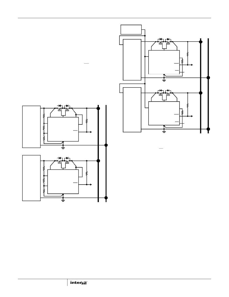
�FIGURE� 49.� CONTROLLED� ON/OFF� APPLICATION� DIAGRAM�
�The� application� diagram� in� Figure� 49� shows� the� ISL6146A� or�
�VOLTAGE�
�DC� -� DC�
�3V-20V�
�+�
�VIN�
�UVLO�
�OVP�
�Q3� Q4�
�GATE�
�ISL6146C�
�GND�
�VOUT�
�ADJ�
�FLT�
�+�
�C�
�O�
�M�
�M�
�O�
�N�
�P�
�O�
�W�
�E�
�R�
�B�
�U�
�S�
�ISL6146B� utilizing� the� EN� or� EN� pin� as� a� signalled� input� to� open�
�or� close� the� conduction� path� from� power� supply� to� load.� This�
�feature� can� be� implemented� on� OR-ing� 1V� to� 20V� but� is� shown�
�for� OR-ing� <3V.�
�The� enable� input� signaling� can� be� simultaneous� across� the� N+1�
�number� of� ISL6146s� used.�
�Although� not� needed� for� thermal� relief,� connect� the� DFN� EPAD�
�to� GND.�
�SWITCH-OVER� CIRCUITS�
�-�
�FIGURE� 48.� TYPICAL� ISL6146C� APPLICATION� DIAGRAM�
�The� ISL6146C� application� shown� in� Figure� 48� is� limited� to� the� 3V�
�to� 20V� V� IN� range� and� must� implement� the� back-to-back� FET�
�configuration� to� utilize� the� UVLO� and� OVP� inputs� and� capabilities.�
�As� the� V� IN� voltage� rises� above� the� minimum� programmed�
�voltage,� the� related� OR-ing� FETs� will� turn� on� and� stay� on� until�
�either� the� minimum� voltage� requirement� is� no� longer� met� or� the�
�V� IN� voltage� exceeds� its� programmed� maximum.� The� minimum�
�and� maximum� programmed� voltage� levels� are� done� with� the�
�resistor� divider� on� the� UVLO� and� OVP� pins.� These� levels� should� be�
�programmed� to� take� into� account� conduction� path� losses� to� the�
�load� in� addition� to� the� IC� operational� constraints.�
�When� using� the� back-to-back� FET� configuration,� the� user� must�
�chose� FETs� to� ensure� (2r� DS(ON)� +� PCB� IR)� I� LOAD� <� 0.5V� to� avoid�
�tripping� the� V� IN� -� V� OUT� >� 0.5V� when� ON� fault.�
�19�
�Switch� over� applications� are� different� than� OR-ing� applications� in�
�that,� the� former� are� looking� for� the� presence� of� or� a� condition� of�
�a� preferred� supply� in� order� to� switch� to� it.� Whereas� true� OR-ing�
�consists� of� a� redundant� N+1� configuration� with� no� preferred�
�source.�
�The� following� 2� circuits� are� simple� single� ISL6146� switchover�
�circuits� optimized� for� situations� particular� to� the� V� BATT� and� V� EXT�
�voltages� relative� to� each� other.� Figure� 50� shows� an� ISL6146B�
�switchover� circuit� where� V� EXT� ,� when� present,� is� the� preferred�
�source� and� V� BATT� could� be� lesser� or� greater� than� V� EXT� .� This� circuit�
�senses� the� presence� of� the� preferred� voltage� supply� to� a�
�programmable� threshold� level� that� when� exceeded,� V� EXT� is�
�passed� to� the� output� as� V� BATT� is� disconnected� from� the� output.�
�R1� &� R2� program� the� V� EXT� level� that� must� be� preset� for� the�
�preferred� voltage� to� be� passed� to� the� output.�
�Q3� is� necessary� if� V� BATT� can� ever� exceed� V� EXT� to� prevent� current�
�from� flowing� into� V� EXT� when� present.� The� body� diode� of� Q3�
�FN7667.4�
�April� 26,� 2013�
�相关PDF资料 |
PDF描述 |
|---|---|
| ISL6146CFRZ-TK | IC OR CONTROLLER |
| ISL6146CFRZ-T | IC OR CONTROLLER |
| ISL6146CFRZ | IC OR CONTROLLER |
| ISL6146BFRZ-TK | IC OR CONTROLLER |
| ISL6146BFRZ-T | IC INTERFACE |
相关代理商/技术参数 |
参数描述 |
|---|---|
| ISL6146AFUZ-T7A | 功能描述:热插拔功率分布 LWV ORING FET CNTRLR 8LD RoHS:否 制造商:Texas Instruments 产品:Controllers & Switches 电流限制: 电源电压-最大:7 V 电源电压-最小:- 0.3 V 工作温度范围: 功率耗散: 安装风格:SMD/SMT 封装 / 箱体:MSOP-8 封装:Tube |
| ISL6146AFUZ-TK | 功能描述:IC OR CTRLR N-CH 1CH 8MSOP RoHS:是 类别:集成电路 (IC) >> PMIC - O 圈控制器 系列:- 标准包装:1,000 系列:- 应用:电池备份,工业/汽车,大电流开关 FET 型:- 输出数:5 内部开关:是 延迟时间 - 开启:100ns 延迟时间 - 关闭:- 电源电压:3 V ~ 5.5 V 电流 - 电源:250µA 工作温度:0°C ~ 70°C 安装类型:表面贴装 封装/外壳:16-SOIC(0.154",3.90mm 宽) 供应商设备封装:16-SOIC N 包装:带卷 (TR) |
| ISL6146B | 制造商:INTERSIL 制造商全称:Intersil Corporation 功能描述:Low Voltage ORing FET Controller |
| ISL6146BEVAL1Z | 制造商:Intersil Corporation 功能描述:ISL6146B EVALUATION BOARD - 8 LEAD - MSOP - ROHS COMPLIANT - Bulk 制造商:Intersil Corporation 功能描述:BOARD EVAL FOR ISL6146 制造商:Intersil 功能描述:ISL98003CNZ-EVALZ EVAL BRD RHS COMPLIA |
| ISL6146BFRZ | 功能描述:IC INTERFACE RoHS:是 类别:集成电路 (IC) >> PMIC - O 圈控制器 系列:* 标准包装:1,000 系列:- 应用:电池备份,工业/汽车,大电流开关 FET 型:- 输出数:5 内部开关:是 延迟时间 - 开启:100ns 延迟时间 - 关闭:- 电源电压:3 V ~ 5.5 V 电流 - 电源:250µA 工作温度:0°C ~ 70°C 安装类型:表面贴装 封装/外壳:16-SOIC(0.154",3.90mm 宽) 供应商设备封装:16-SOIC N 包装:带卷 (TR) |
发布紧急采购,3分钟左右您将得到回复。