- 您现在的位置:买卖IC网 > Datasheet目录333 > ISL6210CRZ (Intersil)IC MOSFET DRIVER DUAL SYNC 16QFN Datasheet资料下载
参数资料
| 型号: | ISL6210CRZ |
| 厂商: | Intersil |
| 文件页数: | 8/10页 |
| 文件大小: | 0K |
| 描述: | IC MOSFET DRIVER DUAL SYNC 16QFN |
| 标准包装: | 75 |
| 配置: | 高端和低端,同步 |
| 输入类型: | PWM |
| 延迟时间: | 26ns |
| 电流 - 峰: | 2A |
| 配置数: | 2 |
| 输出数: | 4 |
| 高端电压 - 最大(自引导启动): | 36V |
| 电源电压: | 4.5 V ~ 5.5 V |
| 工作温度: | -10°C ~ 100°C |
| 安装类型: | 表面贴装 |
| 封装/外壳: | 16-VQFN 裸露焊盘 |
| 供应商设备封装: | 16-QFN-EP(4x4) |
| 包装: | 管件 |
�� �
�
�ISL6210�
�2.0�
�1.8�
�1.6�
�1.4�
�1.2�
�1.0�
�0.8�
�where� the� gate� charge� (Q� G1� and� Q� G2� )� is� defined� at� a�
�particular� gate� to� source� voltage� (V� GS1� and� V� GS2� )� in� the�
�corresponding� MOSFET� data� sheet;� I� Q� is� the� driver� ’s� total�
�quiescent� current� with� no� load� at� both� drive� outputs;� N� Q1�
�and� N� Q2� are� number� of� upper� and� lower� MOSFETs,�
�respectively.� The� I� Q� V� CC� product� is� the� quiescent� power� of�
�the� driver� without� capacitive� load� and� is� typically� negligible.�
�The� total� gate� drive� power� losses� are� dissipated� among� the�
�0.6�
�0.4�
�0.2�
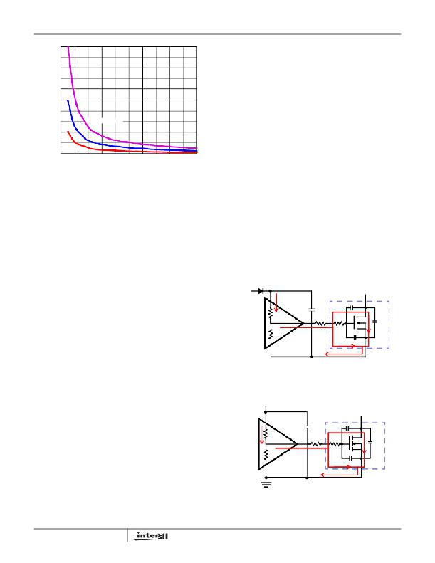
�20nC�
�Q� GATE� = 100nC�
�resistive� components� along� the� transition� path.� The� drive�
�resistance� dissipates� a� portion� of� the� total� gate� drive� power�
�losses,� the� rest� will� be� dissipated� by� the� external� gate�
�resistors� (R� G1� and� R� G2� ,� should� be� a� short� to� avoid�
�0.0�
�0.0� 0.1� 0.2� 0.3� 0.4� 0.5� 0.6� 0.7� 0.8� 0.9� 1.0�
�Δ� V� BOOT_CAP� (V)�
�FIGURE� 4.� BOOTSTRAP� CAPACITANCE� vs� BOOT� RIPPLE�
�VOLTAGE�
�interfering� with� the� operation� shoot-through� protection�
�circuitry)� and� the� internal� gate� resistors� (R� GI1� and� R� GI2� )� of�
�MOSFETs.� Figures� 5� and� 6� show� the� typical� upper� and� lower�
�gate� drives� turn-on� transition� path.� The� power� dissipation� on�
�the� driver� can� be� roughly� estimated� as� follows:�
�P� DR_UP� =� ?� --------------------------------------� +� ----------------------------------------� ?� ?� ---------------------�
�?� R� HI1� +� R� EXT1� R� LO1� +� R� EXT1� ?�
�P� DR_LOW� =� ?� --------------------------------------� +� ----------------------------------------� ?� ?� ---------------------�
�?� R� HI2� +� R� EXT2� R� LO2� +� R� EXT2� ?�
�Power� Dissipation�
�Package� power� dissipation� is� mainly� a� function� of� the�
�switching� frequency� (F� SW� ),� the� output� drive� impedance,� the�
�external� gate� resistance,� and� the� selected� MOSFET’s�
�internal� gate� resistance� and� total� gate� charge.� Calculating�
�the� power� dissipation� in� the� driver� for� a� desired� application� is�
�critical� to� ensure� safe� operation.� Exceeding� the� maximum�
�P� DR� =� P� DR_UP� +� P� DR_LOW� +� I� Q� ?� VCC�
�?� R� HI1� R� LO1� ?� P� Qg_Q1�
�?� R� HI2� R� LO2� ?� P� Qg_Q2�
�2�
�2�
�(EQ.� 6)�
�R� EXT2� =� R� G1� +� -------------�
�N�
�R� EXT2� =� R� G2� +� -------------�
�N�
�allowable� power� dissipation� level� will� push� the� IC� beyond� the�
�maximum� recommended� operating� junction� temperature� of�
�+125°C.� The� maximum� allowable� IC� power� dissipation� for�
�R� GI1�
�Q1�
�R� GI2�
�Q2�
�the� SO14� package� is� approximately� 1W� at� room�
�temperature,� while� the� power� dissipation� capacity� in� the�
�QFN� packages,� with� an� exposed� heat� escape� pad,� is� around�
�2W.� See� “Layout� Considerations”� on� page� 9� for� thermal�
�PVCC�
�BOOT�
�C� GD�
�D�
�transfer� improvement� suggestions.� When� designing� the�
�driver� into� an� application,� it� is� recommended� that� the�
�following� calculation� is� used� to� ensure� safe� operation� at� the�
�R� HI1�
�R� LO1�
�UGATE�
�G�
�R� G1�
�R� GI1�
�C� DS�
�desired� frequency� for� the� selected� MOSFETs.� The� total� gate�
�C� GS�
�Q1�
�drive� power� losses� due� to� the� gate� charge� of� MOSFETs� and�
�the� driver� ’s� internal� circuitry� and� their� corresponding� average�
�driver� current� can� be� estimated� with� Equations� 4� and� 5,�
�respectively,�
�S�
�PHASE�
�FIGURE� 5.� TYPICAL� UPPER-GATE� DRIVE� TURN-ON� PATH�
�P� Qg_TOT� =� P� Qg_Q1� +� P� Qg_Q2� +� I� Q� ?� VCC�
�(EQ.� 4)�
�P� Qg_Q1� =� ---------------------------------------� ?� F� SW� ?� N� Q1�
�Q� G1� ?� PVCC� 2�
�V� GS1�
�PVCC�
�D�
�P� Qg_Q2� =� ---------------------------------------� ?� F� SW� ?� N� Q2�
�Q� G2� ?� PVCC� 2�
�V� GS2�
�R� HI2�
�LGATE�
�G�
�C� GD�
�C� DS�
�R� LO2�
�R� G2�
�R� GI2�
�I� DR� =� ?� ------------------------------� +� ------------------------------� ?� ?� F� SW� +� I� Q�
�?� Q� G1� ?� N� Q1� Q� G2� ?� N� Q2� ?�
�?� V� GS1� V� GS2� ?�
�(EQ.� 5)�
�GND�
�C� GS�
�S�
�Q2�
�FIGURE� 6.� TYPICAL� LOWER-GATE� DRIVE� TURN-ON� PATH�
�8�
�FN6392.1�
�December� 9,� 2008�
�相关PDF资料 |
PDF描述 |
|---|---|
| ISL6244EVAL1 | EVALUATION BOARD ISL6244 |
| ISL6261AEVAL1Z | EVAL BOARD 1 FOR ISL6261A |
| ISL6261EVAL1Z | EVAL BOARD FOR ISL6261 1 QFN |
| ISL6271AEVAL1 | EVALUATION BOARD FOR ISL6271A |
| ISL62882CEVAL2Z | EVAL BOARD FOR ISL62882C |
相关代理商/技术参数 |
参数描述 |
|---|---|
| ISL6210CRZ-T | 功能描述:IC MOSFET DRIVER DUAL SYNC 16QFN RoHS:是 类别:集成电路 (IC) >> PMIC - MOSFET,电桥驱动器 - 外部开关 系列:- 标准包装:50 系列:- 配置:高端 输入类型:非反相 延迟时间:200ns 电流 - 峰:250mA 配置数:1 输出数:1 高端电压 - 最大(自引导启动):600V 电源电压:12 V ~ 20 V 工作温度:-40°C ~ 125°C 安装类型:通孔 封装/外壳:8-DIP(0.300",7.62mm) 供应商设备封装:8-DIP 包装:管件 其它名称:*IR2127 |
| ISL6211 | 制造商:INTERSIL 制造商全称:Intersil Corporation 功能描述:Crusoe⑩ Processor Core-Voltage Regulator |
| ISL6211CA | 制造商:Rochester Electronics LLC 功能描述:CPU REGULATOR FOR TRANSMETA,SINGLE CORE - Bulk 制造商:Intersil Corporation 功能描述: |
| ISL6211CA WAF | 制造商:Intersil Corporation 功能描述: |
| ISL6211CA-T | 制造商:Rochester Electronics LLC 功能描述:CPU REGULATOR FOR TRANSMETA,SINGLE CORE - Tape and Reel 制造商:Intersil Corporation 功能描述: |
发布紧急采购,3分钟左右您将得到回复。