参数资料
| 型号: | ISL6263CHRZ-T |
| 厂商: | Intersil |
| 文件页数: | 11/18页 |
| 文件大小: | 0K |
| 描述: | IC VOLT REG 1PH 5BIT VID 32-QFN |
| 标准包装: | 6,000 |
| 应用: | 转换器,GPU 内核电源 |
| 输入电压: | 5 V ~ 25 V |
| 输出数: | 1 |
| 输出电压: | 0.41 V ~ 1.29 V |
| 工作温度: | -10°C ~ 100°C |
| 安装类型: | 表面贴装 |
| 封装/外壳: | 32-VFQFN 裸露焊盘 |
| 供应商设备封装: | 32-QFN(5x5) |
| 包装: | 带卷 (TR) |
�� �
�
�ISL6263C�
�High� Efficiency� Diode� Emulation� Mode�
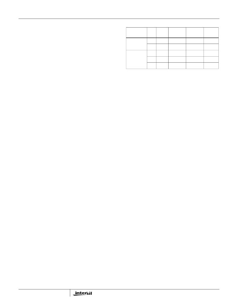
�TABLE� 2.� DIODE� EMULATION� MODE� and� AUDIO� FILTER�
�The� ISL6263C� operates� in� continuous-conduction-mode�
�GPU� MODE�
�DEM�
�VOLTAGE�
�AUDIO�
�(CCM)� during� heavy� load� for� minimum� conduction� loss� by�
�(VID� code)�
�FDE� AF_EN�
�STATUS�
�WINDOW�
�FILTER�
�forcing� the� low-side� MOSFET� to� operate� as� a� synchronous�
�rectifier.� An� improvement� in� light-load� efficiency� is� achieved�
�by� allowing� the� converter� to� operate� in� diode-emulation�
�mode� (DEM)� where� the� low-side� MOSFET� behaves� as� a�
�smart-diode,� forcing� the� device� to� block� negative� inductor�
�current� flow.�
�MODE� 1�
�MODE� 2�
�0�
�1�
�-�
�1�
�0�
�-�
�-�
�0�
�1�
�1�
�DISABLED�
�ENABLED�
�ENABLED�
�ENABLED�
�ENABLED�
�NOM�
�130%� NOM�
�150%� NOM�
�130%� NOM�
�130%� NOM�
�-�
�-�
�-�
�-�
�ENABLED�
�V� IMON� =� (� V� ICOMP� –� V� O� )� ?� 31�
�Positive-going� inductor� current� flows� from� either� the� source�
�of� the� high-side� MOSFET,� or� the� drain� of� the� low-side�
�MOSFET.� Negative-going� inductor� current� flows� into� the�
�source� of� the� high-side� MOSFET,� or� into� the� drain� of� the�
�low-side� MOSFET.� When� the� low-side� MOSFET� conducts�
�positive� inductor� current,� the� phase� voltage� will� be� negative�
�with� respect� to� the� VSS� pin.� Conversely,� when� the� low-side�
�MOSFET� conducts� negative� inductor� current,� the� phase�
�voltage� will� be� positive� with� respect� to� the� VSS� pin.� Negative�
�inductor� current� occurs� when� the� output� DC� load� current� is�
�less� than� ?� the� inductor� ripple� current.� Sinking� negative�
�inductor� current� through� the� low-side� MOSFET� lowers�
�efficiency� through� unnecessary� conduction� losses.� Efficiency�
�can� be� further� improved� with� a� reduction� of� unnecessary�
�switching� losses� by� reducing� the� PWM� frequency.� The� PWM�
�frequency� can� be� configured� to� automatically� make� a�
�step-reduction� upon� entering� DEM� by� forcing� a�
�step-increase� of� the� window� voltage� V� W� .� The� window�
�voltage� can� be� configured� to� increase� approximately� 30%,�
�50%,� or� not� at� all.� The� characteristic� PWM� frequency�
�reduction,� coincident� with� decreasing� load,� is� accelerated� by�
�the� step-increase� of� the� window� voltage.�
�The� converter� will� enter� DEM� after� detecting� three�
�consecutive� PWM� pulses� with� negative� inductor� current.� The�
�negative� inductor� current� is� detected� during� the� time� that� the�
�high-side� MOSFET� gate� driver� output� UGATE� is� low,� with� the�
�exception� of� a� brief� blanking� period.� The� voltage� between�
�the� PHASE� pin� and� VSS� pin� is� monitored� by� a� comparator�
�that� latches� upon� detection� of� positive� phase� voltage.� The�
�converter� will� return� to� CCM� after� detecting� three�
�consecutive� PWM� pulses� with� positive� inductor� current.�
�The� inductor� current� is� considered� positive� if� the� phase�
�comparator� has� not� been� latched� while� UGATE� is� low.�
�Because� the� switching� frequency� in� DEM� is� a� function� of�
�load� current,� very� light� load� condition� can� produce�
�frequencies� well� into� the� audio� band.� To� eliminate� this�
�audible� noise,� an� audio� filter� can� be� enabled� that� briefly� turns�
�on� the� low-side� MOSFET� gate� driver� LGATE� approximately�
�every� 35μs.�
�The� DEM� and� audio� filter� operation� are� programmed� by� the�
�AF_EN� and� FDE� pins� in� conjunction� with� VID0:VID4�
�according� to� Table� 2.�
�11�
�Smooth� mode� transitions� are� facilitated� by� the� R� 3� modulator,�
�which� correctly� maintains� the� internally� synthesized� ripple�
�current� information� throughout� mode� transitions.�
�Current� Monitor�
�The� ISL6263C� features� a� current� monitor� output.� The�
�voltage� between� the� IMON� and� VSS� pins� is� proportional� to�
�the� output� inductor� current.� The� output� inductor� current� is�
�proportional� to� the� voltage� between� the� ICOMP� and� VO� pins.�
�The� IMON� pin� has� source� and� sink� capability� for� close�
�tracking� of� transient� current� events.� The� current� monitor�
�output� is� expressed� in� Equation� 1:�
�(EQ.� 1)�
�Protection�
�The� ISL6263C� provides� overcurrent� protection� (OCP),�
�overvoltage� protection� (OVP),� and� undervoltage� protection�
�(UVP),� as� shown� in� Table� 3.�
�Overcurrent� protection� is� tied� to� the� current� sense� amplifier.�
�Given� the� overcurrent� set� point� I� OC� ,� the� maximum� voltage�
�at� ICOMP� pin� V� ICOMP(max)� (which� is� the� voltage� when�
�OCP� happens)� can� be� determined� by� the� current� sense�
���start-up,� the� ICOMP� pin� must� fall� 25mV� below� the� OCSET�
�pin� to� reset� the� overcurrent� comparator,� which� requires�
�(V� ICOMP(max)� -� V� O� )� >� 25mV.�
�The� OCP� threshold� detector� is� checked� every� 15μs� and� will�
�increment� a� counter� if� the� OCP� threshold� is� exceeded,�
�conversely� the� counter� will� be� decremented� if� the� load�
�current� is� below� the� OCP� threshold.� The� counter� will� latch� an�
�OCP� fault� when� the� counter� reaches� eight.� The� fastest� OCP�
�response� for� overcurrent� levels� that� are� no� more� than� 2.5�
�times� the� OCP� threshold� is� 120μs,� which� is� eight� counts� at�
�15μs� each.� The� ISL6263C� protects� against� hard� shorts� by�
�latching� an� OCP� fault� within� 2μs� for� overcurrent� levels�
�exceeding� 2.5� times� the� OCP� threshold.�
�The� overcurrent� threshold� is� determined� by� the� resistor�
�R� OCSET� between� OCSET� pin� and� VO� pin.� The� value� of�
�R� OCSET� is� calculated� in� Equation� 2:�
�V� ICOMP� (� max� )� –� V� O�
�10� μ� A�
�R� OCSET� =� ----------------------------------------------------� (EQ.� 2)�
�FN6745.1�
�July� 8,� 2010�
�相关PDF资料 |
PDF描述 |
|---|---|
| ISL6263CRZ | IC VREG CORE 5BIT 1PHASE 32-QFN |
| ISL6263DHRZ | IC VREG 3BIT 1PHASE 32-QFN |
| ISL6264CRZ | IC CORE CTRLR TWO-PHASE 40-QFN |
| ISL6265AHRTZ-T | IC CTRLR MULTI-OUTPUT 48-TQFN |
| ISL6265CHRTZ | IC CTRLR MULTI-OUTPUT 48TQFN |
相关代理商/技术参数 |
参数描述 |
|---|---|
| ISL6263CRZ | 功能描述:直流/直流开关调节器 1 PHS INT DC/DC BUCK CNTRLR FOR INTEL RoHS:否 制造商:International Rectifier 最大输入电压:21 V 开关频率:1.5 MHz 输出电压:0.5 V to 0.86 V 输出电流:4 A 输出端数量: 最大工作温度: 安装风格:SMD/SMT 封装 / 箱体:PQFN 4 x 5 |
| ISL6263CRZ-T | 功能描述:直流/直流开关调节器 1 PHS INT DC/DC BUCK CNTRLR FOR INTEL RoHS:否 制造商:International Rectifier 最大输入电压:21 V 开关频率:1.5 MHz 输出电压:0.5 V to 0.86 V 输出电流:4 A 输出端数量: 最大工作温度: 安装风格:SMD/SMT 封装 / 箱体:PQFN 4 x 5 |
| ISL6263DEVAL1Z | 功能描述:EVAL BAORD 1 FOR ISL6263D RoHS:是 类别:编程器,开发系统 >> 评估板 - DC/DC 与 AC/DC(离线)SMPS 系列:* 产品培训模块:Obsolescence Mitigation Program 标准包装:1 系列:True Shutdown™ 主要目的:DC/DC,步升 输出及类型:1,非隔离 功率 - 输出:- 输出电压:- 电流 - 输出:1A 输入电压:2.5 V ~ 5.5 V 稳压器拓扑结构:升压 频率 - 开关:3MHz 板类型:完全填充 已供物品:板 已用 IC / 零件:MAX8969 |
| ISL6263DHRZ | 功能描述:IC VREG 3BIT 1PHASE 32-QFN RoHS:是 类别:集成电路 (IC) >> PMIC - 稳压器 - 专用型 系列:- 产品培训模块:Lead (SnPb) Finish for COTS Obsolescence Mitigation Program 标准包装:2,000 系列:- 应用:电源,ICERA E400,E450 输入电压:4.1 V ~ 5.5 V 输出数:10 输出电压:可编程 工作温度:-40°C ~ 85°C 安装类型:表面贴装 封装/外壳:42-WFBGA,WLCSP 供应商设备封装:42-WLP 包装:带卷 (TR) |
| ISL6263DHRZ-T | 功能描述:IC VREG 3BIT 1PHASE 32-QFN RoHS:是 类别:集成电路 (IC) >> PMIC - 稳压器 - 专用型 系列:- 标准包装:43 系列:- 应用:控制器,Intel VR11 输入电压:5 V ~ 12 V 输出数:1 输出电压:0.5 V ~ 1.6 V 工作温度:-40°C ~ 85°C 安装类型:表面贴装 封装/外壳:48-VFQFN 裸露焊盘 供应商设备封装:48-QFN(7x7) 包装:管件 |
发布紧急采购,3分钟左右您将得到回复。