参数资料
| 型号: | ISL6263CHRZ-T |
| 厂商: | Intersil |
| 文件页数: | 12/18页 |
| 文件大小: | 0K |
| 描述: | IC VOLT REG 1PH 5BIT VID 32-QFN |
| 标准包装: | 6,000 |
| 应用: | 转换器,GPU 内核电源 |
| 输入电压: | 5 V ~ 25 V |
| 输出数: | 1 |
| 输出电压: | 0.41 V ~ 1.29 V |
| 工作温度: | -10°C ~ 100°C |
| 安装类型: | 表面贴装 |
| 封装/外壳: | 32-VFQFN 裸露焊盘 |
| 供应商设备封装: | 32-QFN(5x5) |
| 包装: | 带卷 (TR) |
�� �
�
�ISL6263C�
�For� example,� choose� V� ICOMP(max)� -� V� O� =� 80mV.� R� OCSET�
�can� use� a� 8.06k� ?� resistor,� according� to� Equation� 2.�
�TABLE� 3.� FAULT� PROTECTION� SUMMARY� OF�
�ISL6263C� (Continued)�
�UVP� and� OVP� are� independent� of� the� OCP.� If� the� output�
�voltage� measured� on� the� VO� pin� is� less� than� +300mV� below�
�the� voltage� on� the� SOFT� pin� for� longer� than� 1ms,� the�
�FAULT� TYPE�
�FAULT�
�DURATION�
�PRIOR� TO�
�PROTECTION�
�PROTECTION�
�ACTIONS�
�FAULT�
�RESET�
�controller� will� latch� a� UVP� fault.� If� the� output� voltage�
�measured� on� the� VO� pin� is� >195mV� above� the� voltage� on�
�the� SOFT� pin� for� longer� than� 1ms,� the� controller� will� latch� an�
�OVP� fault.� Keep� in� mind� that� V� SOFT� will� equal� the� voltage�
�level� commanded� by� the� VID� states� only� after� the� soft-start�
�capacitor� C� SOFT� has� slewed� to� the� VID� DAC� output� voltage.�
�The� UVP� and� OVP� detection� circuits� act� on� static� and�
�dynamic� V� SOFT� voltage.�
�When� an� OCP,� OVP,� or� UVP� fault� has� been� latched,� PGOOD�
�Severe�
�Overvoltage�
�(+1.55V)�
�between� VO� pin�
�and� VSS� pin�
�Undervoltage�
�(-300mV)�
�between� VO� pin�
�Immediately�
�1ms�
�UGATE,� and� Cycle�
�PGOOD� latched� low,� VDD� only�
�LGATE� toggles� ON�
�when� VO� >� 1.55V�
�OFF� when�
�VO� <� 0.77V�
�until� fault� reset�
�LGATE,� UGATE,� and� Cycle�
�PGOOD� latched� low� VR_ON� or�
�VDD�
�becomes� a� low� impedance� and� the� gate� driver� outputs�
�UGATE� and� LGATE� are� pulled� low.� The� energy� stored� in� the�
�inductor� is� dissipated� as� current� flows� through� the� low-side�
�MOSFET� body� diode.� The� controller� will� remain� latched� in�
�the� fault� state� until� the� VR_ON� pin� has� been� pulled� below� the�
�falling� VR_ON� threshold� voltage� V� VR_ONL� or� until� VDD� has�
�gone� below� the� falling� POR� threshold� voltage� VVDD_THF� .�
�A� severe-overvoltage� protection� fault� occurs� immediately� after�
�the� voltage� between� the� VO� and� VSS� pins� exceed� the� rising�
�severe-overvoltage� threshold� V� OVPS� which� is� 1.545V,� the�
�same� reference� voltage� used� by� the� VID� DAC.� The� ISL6263C�
�will� latch� UGATE� and� PGOOD� low� but� unlike� other� protective�
�faults,� LGATE� remains� high� until� the� voltage� between� VO� and�
�VSS� falls� below� approximately� 0.77V,� at� which� time� LGATE� is�
�pulled� low.� The� LGATE� pin� will� continue� to� switch� high� and� low�
�at� 1.545V� and� 0.77V� until� VDD� has� gone� below� the� falling�
�POR� threshold� voltage� VVDD_THF.� This� provides� maximum�
�protection� against� a� shorted� high-side� MOSFET� while�
�preventing� the� output� voltage� from� ringing� below� ground.� The�
�severe-overvoltage� fault� circuit� can� be� triggered� after� another�
�and� SOFT� pin�
�Gate-Driver� Outputs� LGATE� and� UGATE�
�The� ISL6263C� has� internal� high-side� and� low-side�
�N-Channel� MOSFET� gate-drivers.� The� LGATE� driver� is�
�optimized� for� low� duty-cycle� applications� where� the� low-side�
�MOSFET� conduction� losses� are� dominant.� The� LGATE�
�pull-down� resistance� is� very� low� in� order� to� clamp� the�
�gate-source� voltage� of� the� MOSFET� below� the� V� GS(th)� at�
�turn-off.� The� current� transient� through� the� low-side� gate� at�
�turn-off� can� be� considerable� due� to� the� characteristic� large�
�switching� charge� of� a� low� r� DS(ON)� MOSFET.�
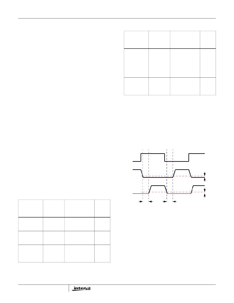
�PWM�
�LGATE�
�1V�
�fault� has� already� been� latched.�
�TABLE� 3.� FAULT� PROTECTION� SUMMARY� OF�
�ISL6263C�
�FAULT�
�DURATION�
�UGATE�
�t� PDRU�
�t� PDRL�
�1V�
�FAULT� TYPE�
�PRIOR� TO�
�PROTECTION�
�PROTECTION�
�ACTIONS�
�FAULT�
�RESET�
�FIGURE� 6.� GATE� DRIVER� TIMING� DIAGRAM�
�Overcurrent�
�Short� Circuit�
�Overvoltage�
�(+195mV)�
�between� VO� pin�
�and� SOFT� pin�
�120μs�
�<2μs�
�1ms�
�LGATE,� UGATE,� and� Cycle�
�PGOOD� latched� low� VR_ON� or�
�VDD�
�LGATE,� UGATE,� and� Cycle�
�PGOOD� latched� low� VR_ON� or�
�VDD�
�LGATE,� UGATE,� and� Cycle�
�PGOOD� latched� low� VR_ON� or�
�VDD�
�Adaptive� shoot-through� protection� prevents� the� gate-driver�
�outputs� from� going� high� until� the� opposite� gate-driver� output�
�has� fallen� below� approximately� 1V.� The� UGATE� turn-on�
�propagation� delay� t� PDRU� and� LGATE� turn-on� propagation�
�delay� t� PDRL� are� found� in� the� “Electrical� Specifications”� table�
�on� page� 6.� The� power� for� the� LGATE� gate-driver� is� sourced�
�directly� from� the� PVCC� pin.� The� power� for� the� UGATE�
�gate-driver� is� sourced� from� a� boot-strap� capacitor� connected�
�across� the� BOOT� and� PHASE� pins.� The� boot� capacitor� is�
�charged� from� PVCC� through� an� internal� boot-strap� diode�
�each� time� the� low-side� MOSFET� turns� on,� pulling� the�
�PHASE� pin� low.�
�12�
�FN6745.1�
�July� 8,� 2010�
�相关PDF资料 |
PDF描述 |
|---|---|
| ISL6263CRZ | IC VREG CORE 5BIT 1PHASE 32-QFN |
| ISL6263DHRZ | IC VREG 3BIT 1PHASE 32-QFN |
| ISL6264CRZ | IC CORE CTRLR TWO-PHASE 40-QFN |
| ISL6265AHRTZ-T | IC CTRLR MULTI-OUTPUT 48-TQFN |
| ISL6265CHRTZ | IC CTRLR MULTI-OUTPUT 48TQFN |
相关代理商/技术参数 |
参数描述 |
|---|---|
| ISL6263CRZ | 功能描述:直流/直流开关调节器 1 PHS INT DC/DC BUCK CNTRLR FOR INTEL RoHS:否 制造商:International Rectifier 最大输入电压:21 V 开关频率:1.5 MHz 输出电压:0.5 V to 0.86 V 输出电流:4 A 输出端数量: 最大工作温度: 安装风格:SMD/SMT 封装 / 箱体:PQFN 4 x 5 |
| ISL6263CRZ-T | 功能描述:直流/直流开关调节器 1 PHS INT DC/DC BUCK CNTRLR FOR INTEL RoHS:否 制造商:International Rectifier 最大输入电压:21 V 开关频率:1.5 MHz 输出电压:0.5 V to 0.86 V 输出电流:4 A 输出端数量: 最大工作温度: 安装风格:SMD/SMT 封装 / 箱体:PQFN 4 x 5 |
| ISL6263DEVAL1Z | 功能描述:EVAL BAORD 1 FOR ISL6263D RoHS:是 类别:编程器,开发系统 >> 评估板 - DC/DC 与 AC/DC(离线)SMPS 系列:* 产品培训模块:Obsolescence Mitigation Program 标准包装:1 系列:True Shutdown™ 主要目的:DC/DC,步升 输出及类型:1,非隔离 功率 - 输出:- 输出电压:- 电流 - 输出:1A 输入电压:2.5 V ~ 5.5 V 稳压器拓扑结构:升压 频率 - 开关:3MHz 板类型:完全填充 已供物品:板 已用 IC / 零件:MAX8969 |
| ISL6263DHRZ | 功能描述:IC VREG 3BIT 1PHASE 32-QFN RoHS:是 类别:集成电路 (IC) >> PMIC - 稳压器 - 专用型 系列:- 产品培训模块:Lead (SnPb) Finish for COTS Obsolescence Mitigation Program 标准包装:2,000 系列:- 应用:电源,ICERA E400,E450 输入电压:4.1 V ~ 5.5 V 输出数:10 输出电压:可编程 工作温度:-40°C ~ 85°C 安装类型:表面贴装 封装/外壳:42-WFBGA,WLCSP 供应商设备封装:42-WLP 包装:带卷 (TR) |
| ISL6263DHRZ-T | 功能描述:IC VREG 3BIT 1PHASE 32-QFN RoHS:是 类别:集成电路 (IC) >> PMIC - 稳压器 - 专用型 系列:- 标准包装:43 系列:- 应用:控制器,Intel VR11 输入电压:5 V ~ 12 V 输出数:1 输出电压:0.5 V ~ 1.6 V 工作温度:-40°C ~ 85°C 安装类型:表面贴装 封装/外壳:48-VFQFN 裸露焊盘 供应商设备封装:48-QFN(7x7) 包装:管件 |
发布紧急采购,3分钟左右您将得到回复。