参数资料
| 型号: | ISL6323BCRZ-T |
| 厂商: | Intersil |
| 文件页数: | 13/36页 |
| 文件大小: | 0K |
| 描述: | IC PWM CTRLR SYNC BUCK DL 48QFN |
| 标准包装: | 4,000 |
| 应用: | 控制器,AMD SVI |
| 输入电压: | 5 V ~ 12 V |
| 输出数: | 2 |
| 输出电压: | 最高 2V |
| 工作温度: | 0°C ~ 70°C |
| 安装类型: | 表面贴装 |
| 封装/外壳: | 48-VFQFN 裸露焊盘 |
| 供应商设备封装: | 48-QFN(7x7) |
| 包装: | 带卷 (TR) |
第1页第2页第3页第4页第5页第6页第7页第8页第9页第10页第11页第12页当前第13页第14页第15页第16页第17页第18页第19页第20页第21页第22页第23页第24页第25页第26页第27页第28页第29页第30页第31页第32页第33页第34页第35页第36页
�� �
�
�ISL6323B�
�L� f� S� V�
�(� V� IN� –� N� V� OUT� )� V� OUT�
�I� C� ,� PP� =� ------------------------------------------------------------�
�IN�
�(EQ.� 3)�
�transitioned� high.� This� is� important� because� it� allows� the�
�controller� to� quickly� respond� to� output� voltage� drops�
�associated� with� current� load� spikes,� while� avoiding� the� ring�
�Another� benefit� of� interleaving� is� to� reduce� input� ripple�
�current.� Input� capacitance� is� determined� in� part� by� the�
�maximum� input� ripple� current.� Multi-phase� topologies� can�
�improve� overall� system� cost� and� size� by� lowering� input� ripple�
�current� and� allowing� the� designer� to� reduce� the� cost� of� input�
�capacitance.� The� example� in� Figure� 2� illustrates� input�
�currents� from� a� three-phase� converter� combining� to� reduce�
�the� total� input� ripple� current.�
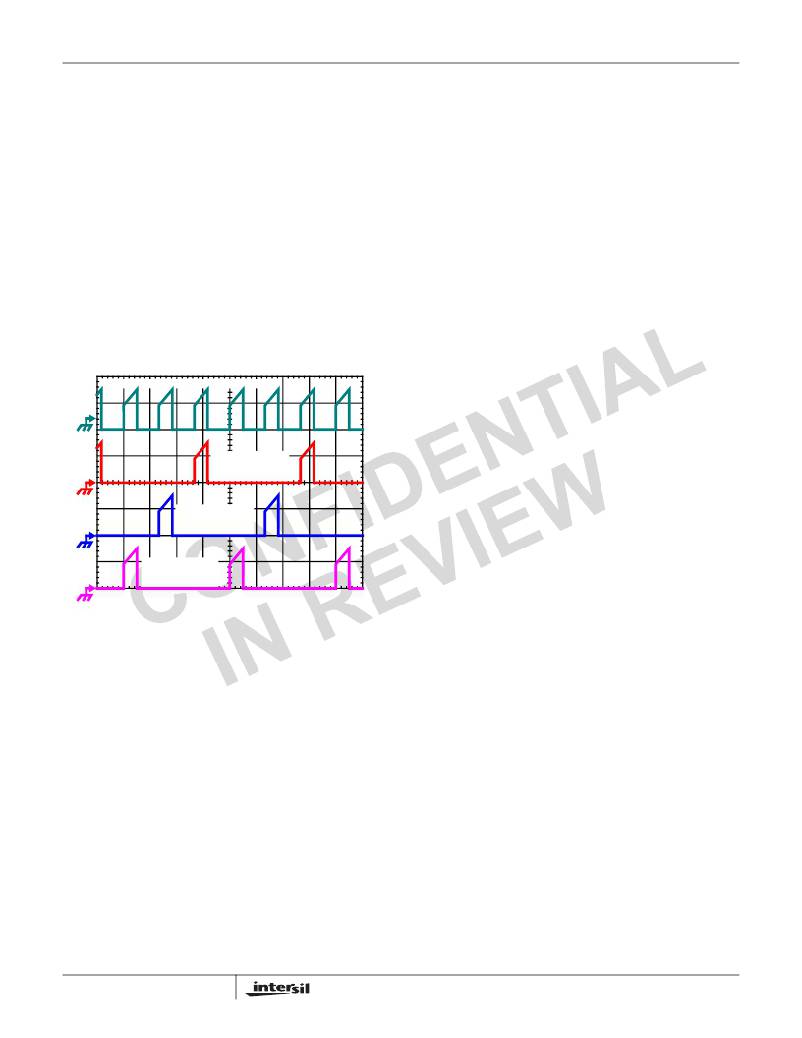
�The� converter� depicted� in� Figure� 2� delivers� 1.5V� to� a� 36A� load�
�from� a� 12V� input.� The� RMS� input� capacitor� current� is� 5.9A.�
�Compare� this� to� a� single-phase� converter� also� stepping� down�
�12V� to� 1.5V� at� 36A.� The� single-phase� converter� has�
�11.9A� RMS� input� capacitor� current.� The� single-phase� converter�
�must� use� an� input� capacitor� bank� with� twice� the� RMS� current�
�capacity� as� the� equivalent� three-phase� converter.�
�INPUT-CAPACITOR CURRENT, 10A/DIV�
�CHANNEL� 3�
�INPUT� CURRENT�
�10A/DIV�
�back� affects� associated� with� other� modulation� schemes.�
�The� PWM� output� state� is� driven� by� the� position� of� the� error�
�amplifier� output� signal,� V� COMP� ,� minus� the� current� correction�
�signal� relative� to� the� proprietary� modulator� ramp� waveform�
�as� illustrated� in� Figure� 3.� At� the� beginning� of� each� PWM� time�
�interval,� this� modified� V� COMP� signal� is� compared� to� the�
�internal� modulator� waveform.� As� long� as� the� modified�
�V� COMP� voltage� is� lower� then� the� modulator� waveform�
�voltage,� the� PWM� signal� is� commanded� low.� The� internal�
�MOSFET� driver� detects� the� low� state� of� the� PWM� signal� and�
�turns� off� the� upper� MOSFET� and� turns� on� the� lower�
�synchronous� MOSFET.� When� the� modified� V� COMP� voltage�
�crosses� the� modulator� ramp,� the� PWM� output� transitions�
�high,� turning� off� the� synchronous� MOSFET� and� turning� on�
�the� upper� MOSFET.� The� PWM� signal� will� remain� high� until�
�the� modified� V� COMP� voltage� crosses� the� modulator� ramp�
�again.� When� this� occurs� the� PWM� signal� will� transition� low�
�again.�
�During� each� PWM� time� interval� the� PWM� signal� can� only�
�transition� high� once.� Once� PWM� transitions� high� it� can� not�
�transition� high� again� until� the� beginning� of� the� next� PWM�
�time� interval.� This� prevents� the� occurrence� of� double� PWM�
�pulses� occurring� during� a� single� period.�
�CHANNEL� 2�
�INPUT� CURRENT�
�10A/DIV�
�CHANNEL� 1�
�INPUT� CURRENT�
�10A/DIV�
�1μs/DIV�
�FIGURE� 2.� CHANNEL� INPUT� CURRENTS� AND� INPUT-�
�CAPACITOR� RMS� CURRENT� FOR� 3-PHASE�
�CONVERTER�
�Figures� 25,� 26� and� 27� in� the� section� entitled� “”� on� page� 33�
�can� be� used� to� determine� the� input-capacitor� RMS� current�
�based� on� load� current,� duty� cycle,� and� the� number� of�
�channels.� They� are� provided� as� aids� in� determining� the�
�optimal� input� capacitor� solution.�
�Active� Pulse� Positioning� Modulated� PWM�
�Operation�
�The� ISL6323B� uses� a� proprietary� Active� Pulse� Positioning�
�(APP)� modulation� scheme� to� control� the� internal� PWM�
�signals� that� command� each� channel’s� driver� to� turn� their�
�upper� and� lower� MOSFETs� on� and� off.� The� time� interval� in�
�which� a� PWM� signal� can� occur� is� generated� by� an� internal�
�clock,� whose� cycle� time� is� the� inverse� of� the� switching�
�frequency� set� by� the� resistor� between� the� FS� pin� and�
�ground.� The� advantage� of� Intersil’s� proprietary� Active� Pulse�
�Positioning� (APP)� modulator� is� that� the� PWM� signal� has� the�
�ability� to� turn� on� at� any� point� during� this� PWM� time� interval,�
�and� turn� off� immediately� after� the� PWM� signal� has�
�13�
�To� further� improve� the� transient� response,� ISL6323B� also�
�implements� Intersil’s� proprietary� Adaptive� Phase� Alignment�
�(APA)� technique,� which� turns� on� all� phases� together� under�
�transient� events� with� large� step� current.� With� both� APP� and�
�APA� control,� ISL6323B� can� achieve� excellent� transient�
�performance� and� reduce� the� demand� on� the� output�
�capacitors.�
�Adaptive� Phase� Alignment� (APA)�
�To� further� improve� the� transient� response,� the� ISL6323B�
�also� implements� Intersil’s� proprietary� Adaptive� Phase�
�Alignment� (APA)� technique,� which� turns� on� all� of� the�
�channels� together� at� the� same� time� during� large� current� step�
�transient� events.� As� Figure� 3� shows,� the� APA� circuitry� works�
�by� monitoring� the� voltage� on� the� APA� pin� and� comparing� it� to�
�a� filtered� copy� of� the� voltage� on� the� COMP� pin.� The� voltage�
�on� the� APA� pin� is� a� copy� of� the� COMP� pin� voltage� that� has�
�been� negatively� offset.� If� the� APA� pin� exceeds� the� filtered�
�COMP� pin� voltage� an� APA� event� occurs� and� all� of� the�
�channels� are� forced� on.�
�FN6879.1�
�May� 12,� 2010�
�相关PDF资料 |
PDF描述 |
|---|---|
| ISL6323ACRZ-T | IC PWM CTRLR SYNC BUCK DL 48QFN |
| ESM36DRSH | CONN EDGECARD 72POS DIP .156 SLD |
| LT1529CQ-3.3#PBF | IC REG LDO 3.3V 3A DDPAK-5 |
| LT1764AET-3.3#PBF | IC REG LDO 3.3V 3A TO220-5 |
| ISL6323CRZ-T | IC HYBRID CTRLR PWM MONO 48-QFN |
相关代理商/技术参数 |
参数描述 |
|---|---|
| ISL6323BCRZ-TR5381 | 制造商:Intersil Corporation 功能描述:4+1 PHASE CONT. FOR CORE+NORTHBRIDGE, 2 PHASE PSI, 3.4MHZ S - Tape and Reel 制造商:Intersil Corporation 功能描述:IC PWM CTRLR SYNC BUCK DL 48QFN 制造商:Intersil 功能描述:4+1 PHS CONT CORE + NORTHBRDG PROG |
| ISL6323BCRZ-TR5453 | 制造商:Intersil Corporation 功能描述:STD. ISL6323BCRZ-T WITH GOLD BOND WIRE ONLY, T&R - Tape and Reel |
| ISL6323BIRZ | 功能描述:IC PWM CTRLR SYNC BUCK DL 48QFN RoHS:是 类别:集成电路 (IC) >> PMIC - 稳压器 - 专用型 系列:- 标准包装:43 系列:- 应用:控制器,Intel VR11 输入电压:5 V ~ 12 V 输出数:1 输出电压:0.5 V ~ 1.6 V 工作温度:-40°C ~ 85°C 安装类型:表面贴装 封装/外壳:48-VFQFN 裸露焊盘 供应商设备封装:48-QFN(7x7) 包装:管件 |
| ISL6323BIRZR5381 | 制造商:Intersil Corporation 功能描述:4+1 PHASE CONT. FOR CORE+NORTHBRIDGE, 2 PHASE PSI, 3.4MHZ SV - Rail/Tube 制造商:Intersil Corporation 功能描述:IC PWM CTRLR SYNC BUCK DL 48QFN 制造商:Intersil 功能描述:4+1 PHS CONT CORE + NORTHBRDG PROG |
| ISL6323BIRZ-T | 功能描述:IC PWM CTRLR SYNC BUCK DL 48QFN RoHS:是 类别:集成电路 (IC) >> PMIC - 稳压器 - 专用型 系列:- 标准包装:43 系列:- 应用:控制器,Intel VR11 输入电压:5 V ~ 12 V 输出数:1 输出电压:0.5 V ~ 1.6 V 工作温度:-40°C ~ 85°C 安装类型:表面贴装 封装/外壳:48-VFQFN 裸露焊盘 供应商设备封装:48-QFN(7x7) 包装:管件 |
发布紧急采购,3分钟左右您将得到回复。