- 您现在的位置:买卖IC网 > PDF目录16598 > ISL6441IR-T (Intersil)IC CTRLR PWM DUAL 1.4MHZ 28-QFN PDF资料下载
参数资料
| 型号: | ISL6441IR-T |
| 厂商: | Intersil |
| 文件页数: | 12/18页 |
| 文件大小: | 0K |
| 描述: | IC CTRLR PWM DUAL 1.4MHZ 28-QFN |
| 标准包装: | 6,000 |
| 应用: | 电源 |
| 电流 - 电源: | 2mA |
| 电源电压: | 5.6 V ~ 24 V |
| 工作温度: | -40°C ~ 85°C |
| 安装类型: | 表面贴装 |
| 封装/外壳: | 28-VFQFN 裸露焊盘 |
| 供应商设备封装: | 28-QFN 裸露焊盘(5x5) |
| 包装: | 带卷 (TR) |
�� �
�
�ISL6441�
�requirements� for� EMI.� The� typical� operating� curves� show� the�
�synchronized� 180� °� out-of-phase� operation.�
�Input� Voltage� Range�
�The� ISL6441� is� designed� to� operate� from� input� supplies�
�ranging� from� 4.5V� to� 24V.� However,� the� input� voltage� range�
�be� too� big.� RBOOT2� only� functions� solely� to� prevent� the�
�overcharge� of� CBOOT.� While� the� RBOOT1� and� RBOOT2�
�will� introduce� voltage� drop� and� reduce� the� DC� voltage� on�
�CBOOT.� So� they� can’t� be� too� large� to� affect� the� DC� driving�
�voltage� of� upper� MOSFET.�
�can� be� effectively� limited� by� the� available� maximum� duty�
�cycle� (D� MAX� =� 71%).�
�VCC_5V�
�DBOOT�
�VIN�
�V� IN� (� min� )� =� ?� --------------------------------� ?� +� V� d2� –� V� d1�
�?� 0.71� ?�
�V� OUT� +� V� d1�
�(EQ.� 3)�
�RBOOT2�
�5.1� Ω�
�CBOOT�
�4.7μF�
�BOOT�
�where,�
�RBOOT1�
�5.1� Ω�
�V� d1� =� Sum� of� the� parasitic� voltage� drops� in� the� inductor�
�discharge� path,� including� the� lower� FET,� inductor� and� PC�
�board.�
�V� d2� =� Sum� of� the� voltage� drops� in� the� charging� path,�
�including� the� upper� FET,� inductor� and� PC� board� resistances.�
�The� maximum� input� voltage� and� minimum� output� voltage� is�
�limited� by� the� minimum� ON-time� (t� ON(min)� ).�
�UGATE�
�PHASE�
�ISL6441�
�CBOOT�
�V� IN� (� max� )� ≤� ----------------------------------------------------�
�V� OUT�
�t� ON� (� min� )� � 1.4MHz�
�(EQ.� 4)�
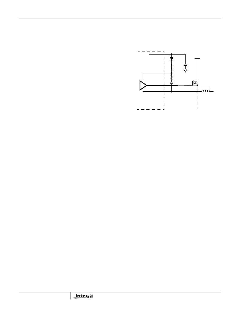
�FIGURE� 15.� GATE� DRIVER�
�At� start-up� the� low-side� MOSFET� turns� on� and� forces�
�(� I� OC� )� (� r� DS� (� ON� )� )�
�where,� t� ON(min)� =� 30ns�
�Gate� Control� Logic�
�The� gate� control� logic� translates� generated� PWM� signals�
�into� gate� drive� signals� providing� amplification,� level� shifting�
�and� shoot-through� protection.� The� gate� drivers� have� some�
�circuitry� that� helps� optimize� the� IC’s� performance� over� a�
�wide� range� of� operational� conditions.� As� MOSFET� switching�
�times� can� vary� dramatically� from� type-to-type� and� with� input�
�voltage,� the� gate� control� logic� provides� adaptive� dead� time�
�by� monitoring� real� gate� waveforms� of� both� the� upper� and� the�
�lower� MOSFETs.� Shoot-through� control� logic� provides� a�
�20ns� deadtime� to� ensure� that� both� the� upper� and� lower�
�MOSFETs� will� not� turn� on� simultaneously� and� cause� a�
�shoot-through� condition.�
�Gate� Drivers�
�The� low-side� gate� driver� is� supplied� from� VCC_5V� and�
�provides� a� peak� sink/source� current� of� 400mA.� The�
�high-side� gate� driver� is� also� capable� of� 400mA� current.�
�Gate-drive� voltages� for� the� upper� N-Channel� MOSFET� are�
�generated� by� the� flying� capacitor� boot� circuit.� A� boot�
�capacitor� (CBOOT� at� Figure� 15)� connected� from� the� BOOT�
�pin� to� the� PHASE� node� provides� power� to� the� high� side�
�MOSFET� driver.� It’s� highly� recommended� to� add� a� small�
�resistor� (RBOOT1� at� Figure� 15,� 5.1� Ω� typical)� in� series� with�
�CBOOT� and� another� small� resistor� (RBOOT2� at� Figure� 15,�
�5.1� Ω� typical)� in� series� with� the� bootstrap� diode� to� prevent� the�
�overcharge� of� CBOOT� that� may� cause� overvoltage� failure�
�between� BOOT� and� PHASE� pin� (Figure� 15).� RBOOT1� also�
�functions� as� the� resistor� in� series� with� the� Ugate� for� damping�
�the� upper� gate� driving� and� phase� node� oscillations,� which�
�helps� to� improves� the� EMI� performance.� But� this� resistor� will�
�slow� down� the� turn-on� of� upper� MOSFET,� so� RBOOT1� can’t�
�12�
�PHASE� to� ground� in� order� to� charge� the� BOOT� capacitor� to�
�5V.� After� the� low-side� MOSFET� turns� off,� the� high-side�
�MOSFET� is� turned� on� by� closing� an� internal� switch� between�
�BOOT� and� UGATE.� This� provides� the� necessary�
�gate-to-source� voltage� to� turn� on� the� upper� MOSFET,� an�
�action� that� boosts� the� 5V� gate� drive� signal� above� V� IN� .� The�
�current� required� to� drive� the� upper� MOSFET� is� drawn� from�
�the� internal� 5V� regulator.�
�Protection� Circuits�
�The� converter� output� is� monitored� and� protected� against�
�overload,� short� circuit� and� undervoltage� conditions.� A�
�sustained� overload� on� the� output� sets� the� PGOOD� low� and�
�initiates� hiccup� mode.�
�Overcurrent� Protection�
�Cycle� by� cycle� current� limiting� scheme� is� implemented� in�
�Equation� 5.� Both� PWM� controllers� use� the� lower� MOSFET’s�
�ON-resistance,� r� DS(ON)� ,� to� monitor� the� current� in� the�
�converter.� The� sensed� voltage� drop� is� compared� with� a�
�threshold� set� by� a� resistor� connected� from� the� OCSETx� pin�
�to� ground.�
�(� 7� )� (� R� CS� )� (EQ.� 5)�
�R� OCSET� =� -------------------------------------------�
�where,� I� OC� is� the� desired� overcurrent� protection� threshold,�
�and� R� CS� is� a� value� of� the� current� sense� resistor� connected�
�to� the� ISENx� pin.� If� the� lower� MOSFET� current� exceeds� the�
�overcurrent� threshold,� a� pulse� skipping� circuit� is� activated.�
�Figure� 16� shows� the� inductor� current,� output� voltage,� and� the�
�PHASE� node� voltage� just� as� an� overcurrent� trip� occurs.� The�
�upper� MOSFET� will� not� be� turned� on� as� long� as� the� sensed�
�current� is� higher� than� the� threshold� value.� This� limits� the�
�current� supplied� by� the� DC� voltage� source.� If� an� overcurrent�
�FN9197.3�
�May� 26,� 2009�
�相关PDF资料 |
PDF描述 |
|---|---|
| RCC05DRYS-S734 | CONN EDGECARD 10POS DIP .100 SLD |
| GSC12DRXH-S734 | CONN EDGECARD 24POS DIP .100 SLD |
| EMC12DREI-S13 | CONN EDGECARD 24POS .100 EXTEND |
| ISL6218CV-T | IC CTRLR INTEL PENT M 38-TSSOP |
| RCM15DCBD | CONN EDGECARD 30POS R/A .156 SLD |
相关代理商/技术参数 |
参数描述 |
|---|---|
| ISL6441IR-TK | 功能描述:IC CTRLR PWM DUAL 1.4MHZ 28-QFN RoHS:否 类别:集成电路 (IC) >> PMIC - 电源管理 - 专用 系列:- 应用说明:Ultrasound Imaging Systems Application Note 产品培训模块:Lead (SnPb) Finish for COTS Obsolescence Mitigation Program 标准包装:37 系列:- 应用:医疗用超声波成像,声纳 电流 - 电源:- 电源电压:2.37 V ~ 6 V 工作温度:0°C ~ 70°C 安装类型:表面贴装 封装/外壳:56-WFQFN 裸露焊盘 供应商设备封装:56-TQFN-EP(8x8) 包装:管件 |
| ISL6441IRZ | 功能描述:IC CTRLR SGL/STEP DOWN PWM 28QFN RoHS:是 类别:集成电路 (IC) >> PMIC - 电源管理 - 专用 系列:- 产品培训模块:Lead (SnPb) Finish for COTS Obsolescence Mitigation Program 标准包装:50 系列:- 应用:热电冷却器 电流 - 电源:- 电源电压:3 V ~ 5.5 V 工作温度:-40°C ~ 85°C 安装类型:表面贴装 封装/外壳:28-SOIC(0.173",4.40mm 宽)裸露焊盘 供应商设备封装:28-TSSOP 裸露焊盘 包装:管件 产品目录页面:1410 (CN2011-ZH PDF) |
| ISL6441IRZS2695 | 制造商:Intersil Corporation 功能描述: |
| ISL6441IRZ-T | 功能描述:IC CTRLR PWM DUAL 1.4MHZ 28-QFN RoHS:是 类别:集成电路 (IC) >> PMIC - 电源管理 - 专用 系列:- 应用说明:Ultrasound Imaging Systems Application Note 产品培训模块:Lead (SnPb) Finish for COTS Obsolescence Mitigation Program 标准包装:37 系列:- 应用:医疗用超声波成像,声纳 电流 - 电源:- 电源电压:2.37 V ~ 6 V 工作温度:0°C ~ 70°C 安装类型:表面贴装 封装/外壳:56-WFQFN 裸露焊盘 供应商设备封装:56-TQFN-EP(8x8) 包装:管件 |
| ISL6441IRZ-TK | 功能描述:IC CTRLR PWM 1.4MHZ DUAL 28-QFN RoHS:是 类别:集成电路 (IC) >> PMIC - 电源管理 - 专用 系列:- 应用说明:Ultrasound Imaging Systems Application Note 产品培训模块:Lead (SnPb) Finish for COTS Obsolescence Mitigation Program 标准包装:37 系列:- 应用:医疗用超声波成像,声纳 电流 - 电源:- 电源电压:2.37 V ~ 6 V 工作温度:0°C ~ 70°C 安装类型:表面贴装 封装/外壳:56-WFQFN 裸露焊盘 供应商设备封装:56-TQFN-EP(8x8) 包装:管件 |
发布紧急采购,3分钟左右您将得到回复。