- 您现在的位置:买卖IC网 > PDF目录16598 > ISL6441IR-T (Intersil)IC CTRLR PWM DUAL 1.4MHZ 28-QFN PDF资料下载
参数资料
| 型号: | ISL6441IR-T |
| 厂商: | Intersil |
| 文件页数: | 14/18页 |
| 文件大小: | 0K |
| 描述: | IC CTRLR PWM DUAL 1.4MHZ 28-QFN |
| 标准包装: | 6,000 |
| 应用: | 电源 |
| 电流 - 电源: | 2mA |
| 电源电压: | 5.6 V ~ 24 V |
| 工作温度: | -40°C ~ 85°C |
| 安装类型: | 表面贴装 |
| 封装/外壳: | 28-VFQFN 裸露焊盘 |
| 供应商设备封装: | 28-QFN 裸露焊盘(5x5) |
| 包装: | 带卷 (TR) |
�� �
�
�ISL6441�
�Due� to� the� current� loop� feedback,� the� modulator� has� a� single�
�pole� response� with� -20� dB� slope� at� a� frequency� determined�
�by� the� load� as� shown� in� Equation� 7.�
�upper� resistor� R� 1� of� the� divider� that� sets� the� output� voltage�
�value.� Please� refer� to� the� “Output� Inductor� Selection”� and�
�the� “Input� Capacitor� Selection� on� page� 17� for� further� details.�
�F� PO� =� ---------------------------------�
�1�
�2� π� ?� R� O� ?� C� O�
�(EQ.� 7)�
�Linear� Regulator�
�where� R� O� is� load� resistance� and� C� O� is� load� capacitance.� For�
�this� type� of� modulator,� a� Type� 2� compensation� circuit� is�
�usually� sufficient.�
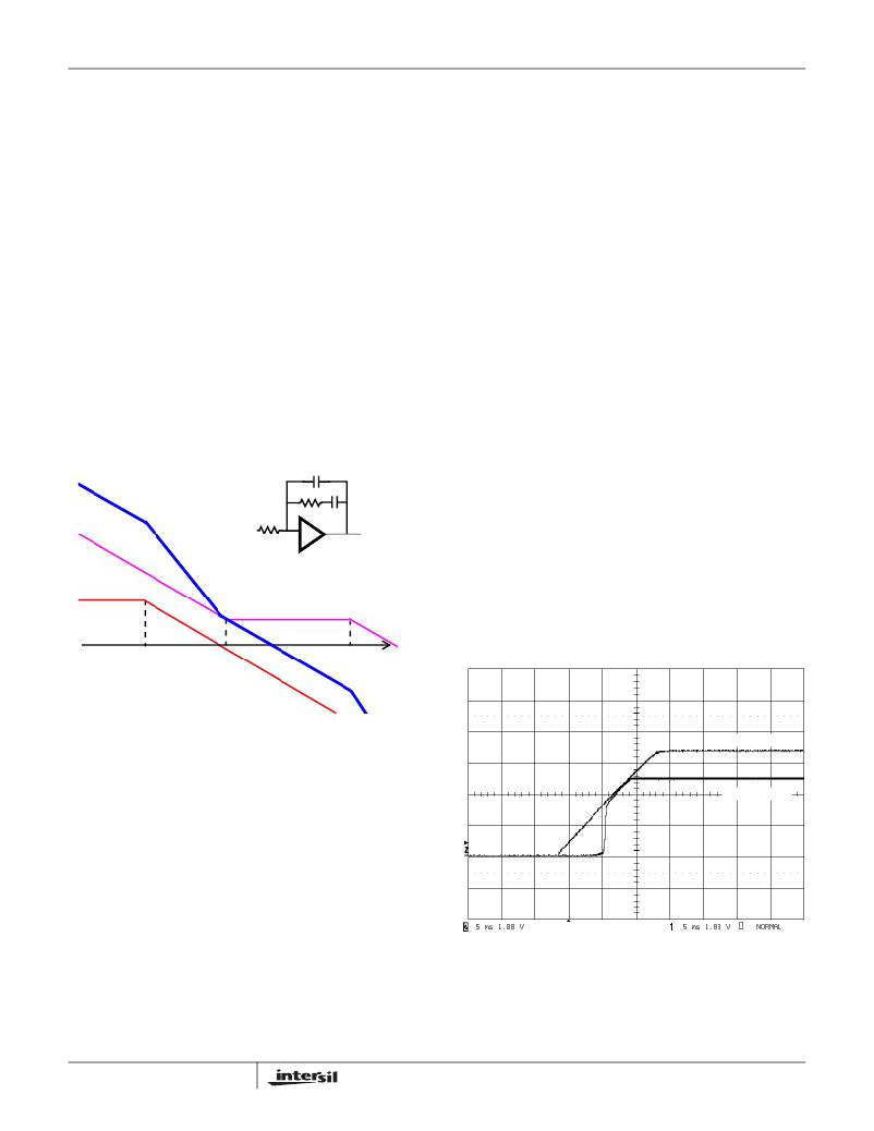
�Figure� 19� shows� a� Type� 2� amplifier� and� it’s� response� along�
�with� the� responses� of� the� current� mode� modulator� and� the�
�converter.� The� Type� 2� amplifier,� in� addition� to� the� pole� at�
�origin,� has� a� zero-pole� pair� that� causes� a� flat� gain� region� at�
�frequencies� in� between� the� zero� and� the� pole� as� shown� in�
�Equations� 8� and� 9.�
�The� linear� regulator� controller� is� a� trans� conductance�
�amplifier� with� a� nominal� gain� of� 2A/V.� The� N-Channel�
�MOSFET� output� device� can� sink� a� minimum� of� 50mA.� The�
�reference� voltage� is� 0.8V.� With� 0V� differential� at� its� input,� the�
�controller� sinks� 21mA� of� current.� An� external� PNP� transistor�
�or� PFET� pass� element� can� be� used.� The� dominant� pole� for�
�the� loop� can� be� placed� at� the� base� of� the� PNP� (or� gate� of� the�
�PFET),� as� a� capacitor� from� emitter� to� base� (source� to� gate� of�
�a� PFET).� Better� load� transient� response� is� achieved�
�however,� if� the� dominant� pole� is� placed� at� the� output,� with� a�
�F� Z� =� -------------------------------� =� 10kHz�
�1�
�F� P� =� =� 600kHz�
�2� π� ?� R� 1� ?� C� 2�
�1�
�2� π� ?� R� 2� ?� C� 1�
�-------------------------------�
�(EQ.� 8)�
�(EQ.� 9)�
�capacitor� to� ground� at� the� output� of� the� regulator.�
�Under� no-load� conditions,� leakage� currents� from� the� pass�
�transistors� supply� the� output� capacitors,� even� when� the�
�transistor� is� off.� Generally� this� is� not� a� problem� since� the�
�feedback� resistor� drains� the� excess� charge.� However,�
�charge� may� build� up� on� the� output� capacitor� making� V� LDO�
�rise� above� its� set� point.� Care� must� be� taken� to� insure� that� the�
�CONVERTER�
�R1�
�R2�
�C2�
�C1�
�feedback� resistor� ’s� current� exceeds� the� pass� transistor� ’s�
�leakage� current� over� the� entire� temperature� range.�
�The� linear� regulator� output� can� be� supplied� by� the� output� of�
�one� of� the� PWMs.� When� using� a� PFET,� the� output� of� the�
�EA�
�G� M� =� 15.5dB�
�MODULATOR�
�F� PO�
�F� Z�
�TYPE� 2� EA�
�G� EA� =13dB�
�F� C�
�F� P�
�linear� will� track� the� PWM� supply� after� the� PWM� output� rises�
�to� a� voltage� greater� than� the� threshold� of� the� PFET� pass�
�device.� The� voltage� differential� between� the� PWM� and� the�
�linear� output� will� be� the� load� current� times� the� r� DS(ON)� .�
�Figure� 20� shows� the� linear� regulator� (2.5V)� start-up�
�waveform� and� the� PWM� (3.3V)� start-up� waveform.�
�FIGURE� 19.� FEEDBACK� LOOP� COMPENSATION�
�V� OUT2� 1V/DIV�
�The� zero� frequency,� the� amplifier� high-frequency� gain,� and�
�the� modulator� gain� are� chosen� to� satisfy� most� typical�
�applications.� The� crossover� frequency� will� appear� at� the�
�point� where� the� modulator� attenuation� equals� the� amplifier�
�high� frequency� gain.� The� only� task� that� the� system� designer�
�has� to� complete� is� to� specify� the� output� filter� capacitors� to�
�position� the� load� main� pole� somewhere� within� one� decade�
�lower� than� the� amplifier� zero� frequency.� With� this� type� of�
�compensation� plenty� of� phase� margin� is� easily� achieved� due�
�to� zero-pole� pair� phase� ‘boost’.�
�Conditional� stability� may� occur� only� when� the� main� load� pole�
�is� positioned� too� much� to� the� left� side� on� the� frequency� axis�
�due� to� excessive� output� filter� capacitance.� In� this� case,� the�
�ESR� zero� placed� within� the� 10kHz� to� 50kHz� range� gives�
�some� additional� phase� ‘boost’.� Some� phase� boost� can� also�
�be� achieved� by� connecting� capacitor� C� Z� in� parallel� with� the�
�14�
�V� OUT3� 1V/DIV�
�FIGURE� 20.� LINEAR� REGULATOR� START-UP� WAVEFORM�
�FN9197.3�
�May� 26,� 2009�
�相关PDF资料 |
PDF描述 |
|---|---|
| RCC05DRYS-S734 | CONN EDGECARD 10POS DIP .100 SLD |
| GSC12DRXH-S734 | CONN EDGECARD 24POS DIP .100 SLD |
| EMC12DREI-S13 | CONN EDGECARD 24POS .100 EXTEND |
| ISL6218CV-T | IC CTRLR INTEL PENT M 38-TSSOP |
| RCM15DCBD | CONN EDGECARD 30POS R/A .156 SLD |
相关代理商/技术参数 |
参数描述 |
|---|---|
| ISL6441IR-TK | 功能描述:IC CTRLR PWM DUAL 1.4MHZ 28-QFN RoHS:否 类别:集成电路 (IC) >> PMIC - 电源管理 - 专用 系列:- 应用说明:Ultrasound Imaging Systems Application Note 产品培训模块:Lead (SnPb) Finish for COTS Obsolescence Mitigation Program 标准包装:37 系列:- 应用:医疗用超声波成像,声纳 电流 - 电源:- 电源电压:2.37 V ~ 6 V 工作温度:0°C ~ 70°C 安装类型:表面贴装 封装/外壳:56-WFQFN 裸露焊盘 供应商设备封装:56-TQFN-EP(8x8) 包装:管件 |
| ISL6441IRZ | 功能描述:IC CTRLR SGL/STEP DOWN PWM 28QFN RoHS:是 类别:集成电路 (IC) >> PMIC - 电源管理 - 专用 系列:- 产品培训模块:Lead (SnPb) Finish for COTS Obsolescence Mitigation Program 标准包装:50 系列:- 应用:热电冷却器 电流 - 电源:- 电源电压:3 V ~ 5.5 V 工作温度:-40°C ~ 85°C 安装类型:表面贴装 封装/外壳:28-SOIC(0.173",4.40mm 宽)裸露焊盘 供应商设备封装:28-TSSOP 裸露焊盘 包装:管件 产品目录页面:1410 (CN2011-ZH PDF) |
| ISL6441IRZS2695 | 制造商:Intersil Corporation 功能描述: |
| ISL6441IRZ-T | 功能描述:IC CTRLR PWM DUAL 1.4MHZ 28-QFN RoHS:是 类别:集成电路 (IC) >> PMIC - 电源管理 - 专用 系列:- 应用说明:Ultrasound Imaging Systems Application Note 产品培训模块:Lead (SnPb) Finish for COTS Obsolescence Mitigation Program 标准包装:37 系列:- 应用:医疗用超声波成像,声纳 电流 - 电源:- 电源电压:2.37 V ~ 6 V 工作温度:0°C ~ 70°C 安装类型:表面贴装 封装/外壳:56-WFQFN 裸露焊盘 供应商设备封装:56-TQFN-EP(8x8) 包装:管件 |
| ISL6441IRZ-TK | 功能描述:IC CTRLR PWM 1.4MHZ DUAL 28-QFN RoHS:是 类别:集成电路 (IC) >> PMIC - 电源管理 - 专用 系列:- 应用说明:Ultrasound Imaging Systems Application Note 产品培训模块:Lead (SnPb) Finish for COTS Obsolescence Mitigation Program 标准包装:37 系列:- 应用:医疗用超声波成像,声纳 电流 - 电源:- 电源电压:2.37 V ~ 6 V 工作温度:0°C ~ 70°C 安装类型:表面贴装 封装/外壳:56-WFQFN 裸露焊盘 供应商设备封装:56-TQFN-EP(8x8) 包装:管件 |
发布紧急采购,3分钟左右您将得到回复。