- 您现在的位置:买卖IC网 > Datasheet目录334 > ISL6442EVAL1Z (Intersil)EVAL BOARD FOR ISL6442 Datasheet资料下载
参数资料
| 型号: | ISL6442EVAL1Z |
| 厂商: | Intersil |
| 文件页数: | 12/16页 |
| 文件大小: | 0K |
| 描述: | EVAL BOARD FOR ISL6442 |
| 标准包装: | 1 |
| 主要目的: | DC/DC,LDO 步降 |
| 输出及类型: | 3,非隔离 |
| 输出电压: | 1.8V,3.3V,5V |
| 电流 - 输出: | 3A,3A,300mA |
| 输入电压: | 6V |
| 稳压器拓扑结构: | 降压 |
| 频率 - 开关: | 1.4MHz |
| 板类型: | 完全填充 |
| 已供物品: | 板 |
| 已用 IC / 零件: | ISL6442 |
�� �
�
�ISL6442�
�High� frequency� decoupling� capacitors� should� be� placed� as�
�close� to� the� power� pins� of� the� load� as� physically� possible.� Be�
�careful� not� to� add� inductance� in� the� circuit� board� wiring� that�
�could� cancel� the� usefulness� of� these� low� inductance�
�components.� Consult� with� the� manufacturer� of� the� load� on�
�specific� decoupling� requirements.� Keep� in� mind� that� not� all�
�applications� have� the� same� requirements;� some� may� need�
�many� ceramic� capacitors� in� parallel;� others� may� need� only� one.�
�Use� only� specialized� low-ESR� capacitors� intended� for�
�switching-regulator� applications� for� the� bulk� capacitors.� The�
�bulk� capacitor� ’s� ESR� will� determine� the� output� ripple� voltage�
�and� the� initial� voltage� drop� after� a� high� slew-rate� transient.�
�An� aluminum� electrolytic� capacitor's� ESR� value� is� related� to�
�the� case� size� with� lower� ESR� available� in� larger� case� sizes.�
�However,� the� equivalent� series� inductance� (ESL)� of� these�
�capacitors� increases� with� case� size� and� can� reduce� the�
�usefulness� of� the� capacitor� to� high� slew-rate� transient� loading.�
�Unfortunately,� ESL� is� not� a� specified� parameter.� Work� with�
�your� capacitor� supplier� and� measure� the� capacitor’s�
�impedance� with� frequency� to� select� a� suitable� component.� In�
�most� cases,� multiple� electrolytic� capacitors� of� small� case� size�
�perform� better� than� a� single� large� case� capacitor.�
�INPUT� CAPACITOR� SELECTION�
�Use� a� mix� of� input� bypass� capacitors� to� control� the� voltage�
�overshoot� across� the� MOSFETs.� Use� small� ceramic�
�capacitors� for� high� frequency� decoupling� and� bulk� capacitors�
�to� supply� the� current� needed� each� time� Q1� (upper� FET)�
�turns� on.� Place� the� small� ceramic� capacitors� physically� close�
�to� the� MOSFETs� and� between� the� drain� of� Q1� and� the� source�
�of� Q2� (lower� FET).�
�The� important� parameters� for� the� bulk� input� capacitor� are� the�
�voltage� rating� and� the� RMS� current� rating.� For� reliable�
�operation,� select� the� bulk� capacitor� with� voltage� and� current�
�ratings� above� the� maximum� input� voltage� and� largest� RMS�
�of� the� regulator� is� a� major� contributor� to� the� overall� IC� power�
�dissipation� (especially� as� C� in� of� the� FET� or� V� IN� or� F� SW�
�increases).�
�Since� V� CC� is� around� 5V,� that� affects� the� FET� selection� in� two�
�ways.� First,� the� FET� gate-source� voltage� rating� (V� GS� )� can� be�
�as� low� as� 12V� (this� rating� is� usually� consistent� with� the� 20V�
�or� 30V� breakdown� chosen� above).� Second,� the� FETs� must�
�have� a� low� threshold� voltage� (around� 1V),� in� order� to� have� its�
�r� DS(ON)� rating� at� V� GS� =� 4.5V� in� the� 10m� Ω� to� 40m� Ω� range�
�that� is� typically� used� for� these� applications.� While� some�
�FETs� are� also� rated� with� gate� voltages� as� low� as� 2.7V,� with�
�typical� thresholds� under� 1V,� these� can� cause� application�
�problems.� As� LGATE� shuts� off� the� lower� FET,� it� does� not�
�take� much� ringing� in� the� LGATE� signal� to� turn� the� lower� FET�
�back� on,� while� the� Upper� FET� is� starting� to� turn� on,� causing�
�some� shoot-through� current.� Therefore,� avoid� FETs� with�
�thresholds� below� 1V.�
�If� the� power� efficiency� of� the� system� is� important,� then� other�
�FET� parameters� are� also� considered.� Efficiency� is� a�
�measure� of� power� losses� from� input� to� output,� and� it�
�contains� two� major� components:� losses� in� the� IC� (mostly� in�
�the� gate� drivers)� and� losses� in� the� FETs.� For� low� duty� cycle�
�applications� (such� as� 12V� in� to� 1.5V� out),� the� upper� FET� is�
�usually� chosen� for� low� gate� charge,� since� switching� losses�
�are� key,� while� the� lower� FET� is� chosen� for� low� r� DS(ON)� ,� since�
�it� is� on� most� of� the� time.� For� high� duty� cycles� (such� as� 5.0V�
�in� to� 3.3V� out),� the� opposite� may� be� true.�
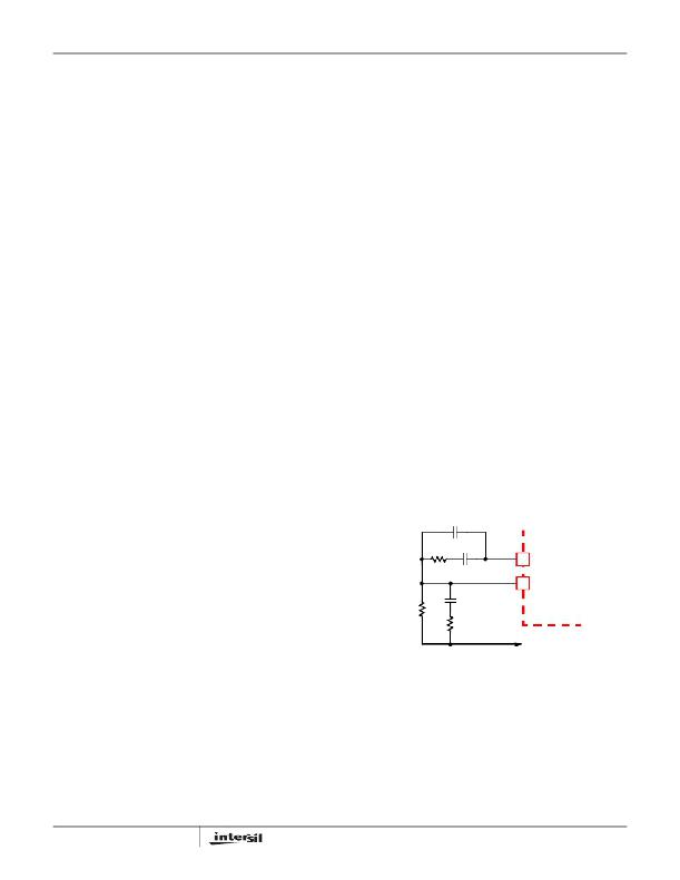
�Feedback� Compensation� Equations�
�This� section� highlights� the� design� consideration� for� a� voltage�
�mode� controller� requiring� external� compensation.� To� address� a�
�broad� range� of� applications,� a� type-3� feedback� network� is�
�recommended� (see� Figure� 13).�
�C2�
�current� required� by� the� circuit.� The� capacitor� voltage� rating�
�should� be� at� least� 1.25� times� greater� than� the� maximum�
�input� voltage� and� a� voltage� rating� of� 1.5� times� is� a�
�R2�
�C1�
�COMP�
�FB�
�conservative� guideline.� The� RMS� current� rating� requirement�
�for� the� input� capacitor� of� a� buck� regulator� is� approximately�
�1/2� the� DC� load� current.�
�R1�
�C3�
�ISL6442�
�R3�
�SWITCHER� MOSFET� SELECTION�
�V� IN� for� the� ISL6442� has� a� wide� operating� voltage� range�
�allowed,� so� both� FETs� should� have� a� source-drain�
�breakdown� voltage� (V� DS� )� above� the� maximum� supply�
�voltage� expected;� 20V� or� 30V� are� typical� values� available.�
�The� ISL6442� gate� drivers� (UGATE� x� and� LGATE� x� )� were�
�designed� to� drive� single� FETs� (for� up� to� ~10A� of� load� current)� or�
�smaller� dual� FETs� (up� to� 4A).� Both� sets� of� drivers� are� sourced�
�by� the� internal� VCC� regulator� (unless� V� IN� =� V� CC� =� 5V,� in� which�
�case� the� gate� driver� current� comes� from� the� external� 5V�
�supply).� The� maximum� current� of� the� regulator� (I� CC_max)� is�
�listed� in� the� “Electrical� Specifications”� Table� on� page� 4;� this� may�
�limit� how� big� the� FETs� can� be.� In� addition,� the� power� dissipation�
�12�
�V� OUT�
�FIGURE� 13.� COMPENSATION� CONFIGURATION� FOR� ISL6442�
�CIRCUIT�
�Figure� 14� highlights� the� voltage-mode� control� loop� for� a�
�synchronous-rectified� buck� converter,� applicable� to� the�
�ISL6442� circuit.� The� output� voltage� (V� OUT� )� is� regulated� to� the�
�reference� voltage,� V� REF� .� The� error� amplifier� output� (COMP� pin�
�voltage)� is� compared� with� the� oscillator� (OSC)� modified�
�sawtooth� wave� to� provide� a� pulse-width� modulated� wave� with�
�an� amplitude� of� V� IN� at� the� PHASE� node.� The� PWM� wave� is�
�smoothed� by� the� output� filter� (L� and� C).� The� output� filter�
�capacitor� bank’s� equivalent� series� resistance� is� represented� by�
�the� series� resistor� E.�
�FN9204.2�
�October� 31,� 2008�
�相关PDF资料 |
PDF描述 |
|---|---|
| ISL6445EVAL3Z | EVALUATION BOARD FOR ISL6445 |
| ISL6524EVAL1 | EVALUATION BOARD VRM8.5 ISL6524 |
| ISL6527EVAL1 | EVALUATION BOARD SOIC ISL6527 |
| ISL6532AEVAL1 | EVALUATION BOARD 1 ISL6532A |
| ISL6553EVAL1 | EVALUATION BOARD ISL6553 |
相关代理商/技术参数 |
参数描述 |
|---|---|
| ISL6442IA | 功能描述:IC REG TRPL BCK/LINEAR 24QSOP RoHS:否 类别:集成电路 (IC) >> PMIC - 稳压器 - 线性 + 切换式 系列:- 标准包装:2,500 系列:- 拓扑:降压(降压)同步(3),线性(LDO)(2) 功能:任何功能 输出数:5 频率 - 开关:300kHz 电压/电流 - 输出 1:控制器 电压/电流 - 输出 2:控制器 电压/电流 - 输出 3:控制器 带 LED 驱动器:无 带监控器:无 带序列发生器:是 电源电压:5.6 V ~ 24 V 工作温度:-40°C ~ 85°C 安装类型:* 封装/外壳:* 供应商设备封装:* 包装:* |
| ISL6442IA-TK | 功能描述:IC REG TRPL BCK/LINEAR 24QSOP RoHS:否 类别:集成电路 (IC) >> PMIC - 稳压器 - 线性 + 切换式 系列:- 标准包装:2,500 系列:- 拓扑:降压(降压)同步(3),线性(LDO)(2) 功能:任何功能 输出数:5 频率 - 开关:300kHz 电压/电流 - 输出 1:控制器 电压/电流 - 输出 2:控制器 电压/电流 - 输出 3:控制器 带 LED 驱动器:无 带监控器:无 带序列发生器:是 电源电压:5.6 V ~ 24 V 工作温度:-40°C ~ 85°C 安装类型:* 封装/外壳:* 供应商设备封装:* 包装:* |
| ISL6442IAZ | 功能描述:IC REG TRPL BCK/LINEAR 24QSOP RoHS:是 类别:集成电路 (IC) >> PMIC - 稳压器 - 线性 + 切换式 系列:- 标准包装:2,500 系列:- 拓扑:降压(降压)同步(3),线性(LDO)(2) 功能:任何功能 输出数:5 频率 - 开关:300kHz 电压/电流 - 输出 1:控制器 电压/电流 - 输出 2:控制器 电压/电流 - 输出 3:控制器 带 LED 驱动器:无 带监控器:无 带序列发生器:是 电源电压:5.6 V ~ 24 V 工作温度:-40°C ~ 85°C 安装类型:* 封装/外壳:* 供应商设备封装:* 包装:* |
| ISL6442IAZ-TK | 功能描述:IC REG TRPL BCK/LINEAR 24QSOP RoHS:是 类别:集成电路 (IC) >> PMIC - 稳压器 - 线性 + 切换式 系列:- 标准包装:2,500 系列:- 拓扑:降压(降压)同步(3),线性(LDO)(2) 功能:任何功能 输出数:5 频率 - 开关:300kHz 电压/电流 - 输出 1:控制器 电压/电流 - 输出 2:控制器 电压/电流 - 输出 3:控制器 带 LED 驱动器:无 带监控器:无 带序列发生器:是 电源电压:5.6 V ~ 24 V 工作温度:-40°C ~ 85°C 安装类型:* 封装/外壳:* 供应商设备封装:* 包装:* |
| ISL6442IAZ-TKS2715 | 制造商:Intersil Corporation 功能描述:BROADCOM, ISL6442IAZ-TK BUSINESS TRACKING REQUIREMENTS, SOLD - Tape and Reel |
发布紧急采购,3分钟左右您将得到回复。