- 您现在的位置:买卖IC网 > PDF目录16722 > ISL6504CBZ-T (Intersil)IC PWR SUPPLY CTRLR/MONTR 16SOIC PDF资料下载
参数资料
| 型号: | ISL6504CBZ-T |
| 厂商: | Intersil |
| 文件页数: | 12/16页 |
| 文件大小: | 0K |
| 描述: | IC PWR SUPPLY CTRLR/MONTR 16SOIC |
| 标准包装: | 1,000 |
| 应用: | 电源控制器/监控器 |
| 电源电压: | 4.75 V ~ 5.25 V |
| 电流 - 电源: | 17mA |
| 工作温度: | 0°C ~ 70°C |
| 安装类型: | 表面贴装 |
| 封装/外壳: | 16-SOIC(0.295",7.50mm 宽) |
| 供应商设备封装: | 16-SOIC |
| 包装: | 带卷 (TR) |
�� �
�
�ISL6504,� ISL6504A�
�pins� of� the� control� IC,� and� connect� them� to� ground� through� a�
�via� placed� close� to� the� ground� pad.� Minimize� any� leakage�
�current� paths� from� the� SS� node,� as� the� internal� current�
�source� is� only� 10� μ� A� (typical).�
�+12VIN�
�+5VSB�
�high� quality� capacitors� to� supply� the� high� slew� rate� (di/dt)�
�current� demands.� Thus,� it� is� recommended� that� the� output�
�capacitors� be� selected� for� transient� load� regulation,� paying�
�attention� to� their� parasitic� components� (ESR,� ESL).�
�Also,� during� the� transition� between� active� and� sleep� states�
�on� the� 3.3V� DUAL� /3.3V� SB� and� 5V� DUAL� outputs,� there� is� a�
�C5VSB�
�CIN�
�short� interval� of� time� during� which� none� of� the� power� pass�
�CHF1�
�t� t�
�?� V� OUT� =� I� OUT� � ?� ESR� OUT� +� ----------------� ?� ,� where�
�CSS�
�CBULK1�
�VOUT1�
�SS�
�1V5SB�
�5VSB�
�5VDLSB�
�5VDL�
�CBULK4�
�Q3�
�VOUT4�
�CHF4�
�elements� are� conducting� -� during� this� time� the� output�
�capacitors� have� to� supply� all� the� output� current.� The� output�
�voltage� drop� during� this� brief� period� of� time� can� be� easily�
�approximated� with� the� following� formula:�
�?� ?�
�?� C� OUT� ?�
�Q1�
�3V3DLSB�
�?� V� OUT� -� output� voltage� drop�
�CHF3�
�VOUT3�
�CBULK3�
�DLA�
�3V3DL�
�ISL6504/A�
�1V2VID�
�Q4�
�+5VIN�
�CBULK2�
�VOUT2�
�ESR� OUT� -� output� capacitor� bank� ESR�
�I� OUT� -� output� current� during� transition�
�C� OUT� -� output� capacitor� bank� capacitance�
�t� t� -� active-to-sleep� or� sleep-to-active� transition� time� (10� μ� s� typ.)�
�The� output� voltage� drop� is� heavily� dependent� on� the� ESR�
�Q2�
�3V3�
�GND�
�CHF2�
�(equivalent� series� resistance)� of� the� output� capacitor� bank,�
�the� choice� of� capacitors� should� be� such� as� to� maintain� the�
�output� voltage� above� the� lowest� allowable� regulation� level.�
�+3.3VIN�
�Input� Capacitors� Selection�
�The� input� capacitors� for� an� ISL6504/A� application� must� have�
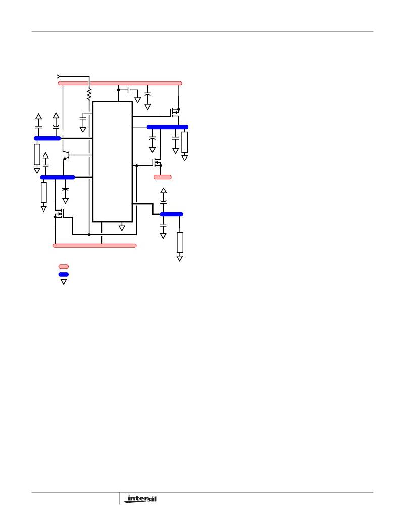
�KEY�
�ISLAND� ON� POWER� PLANE� LAYER�
�ISLAND� ON� CIRCUIT/POWER� PLANE� LAYER�
�VIA� CONNECTION� TO� GROUND� PLANE�
�a� sufficiently� low� ESR� so� as� not� to� allow� the� input� voltage� to�
�dip� excessively� when� energy� is� transferred� to� the� output�
�capacitors.� If� the� ATX� supply� does� not� meet� the�
�specifications,� certain� imbalances� between� the� ATX’s�
�FIGURE� 11.� PRINTED� CIRCUIT� BOARD� ISLANDS�
�A� multi-layer� printed� circuit� board� is� recommended.�
�Figure� 11� shows� the� connections� to� most� of� the� components�
�in� the� circuit.� Note� that� the� individual� capacitors� shown� each�
�could� represent� numerous� physical� capacitors.� Dedicate� one�
�solid� layer� for� a� ground� plane� and� make� all� critical�
�component� ground� connections� through� vias� placed� as� close�
�to� the� component� terminal� as� possible.� Dedicate� another�
�solid� layer� as� a� power� plane� and� break� this� plane� into�
�smaller� islands� of� common� voltage� levels.� Ideally,� the� power�
�plane� should� support� both� the� input� power� and� output� power�
�nodes.� Use� copper� filled� polygons� on� the� top� and� bottom�
�circuit� layers� to� create� power� islands� connecting� the� filtering�
�components� (output� capacitors)� and� the� loads.� Use� the�
�remaining� printed� circuit� layers� for� small� signal� wiring.�
�Component� Selection� Guidelines�
�Output� Capacitors� Selection�
�The� output� capacitors� should� be� selected� to� allow� the� output�
�voltage� to� meet� the� dynamic� regulation� requirements� of�
�active� state� operation� (S0,� S1).� The� load� transient� for� the�
�various� microprocessor� system’s� components� may� require�
�12�
�outputs� and� the� ISL6504/A’s� regulation� levels� could� have� as�
�a� result� a� brisk� transfer� of� energy� from� the� input� capacitors� to�
�the� supplied� outputs.� At� the� transition� between� active� and�
�sleep� states,� such� phenomena� could� be� responsible� for� the�
�5V� SB� voltage� drooping� excessively� and� affecting� the� output�
�regulation.� The� solution� to� such� a� potential� problem� is� using�
�larger� input� capacitors� with� a� lower� total� combined� ESR.�
�Transistor� Selection/Considerations�
�The� ISL6504/A� usually� requires� one� P-Channel� (or� bipolar�
�PNP),� two� N-Channel� MOSFETs,� and� one� bipolar� NPN�
�transistors.�
�One� important� criteria� for� selection� of� transistors� for� all� the�
�linear� regulators/switching� elements� is� package� selection� for�
�efficient� removal� of� heat.� The� power� dissipated� in� a� linear�
�regulator� or� an� ON/OFF� switching� element� is�
�P� LINEAR� =� I� O� ×� (� V� IN� –� V� OUT� )�
�Select� a� package� and� heatsink� that� maintains� the� junction�
�temperature� below� the� rating� with� the� maximum� expected�
�ambient� temperature.�
�FN9062.2�
�April� 13,� 2004�
�相关PDF资料 |
PDF描述 |
|---|---|
| REC5-4812DRW/H4/C | CONV DC/DC 5W 36-72VIN +/-12VOUT |
| RBM18DCSN | CONN EDGECARD 36POS DIP .156 SLD |
| PCV1D470MCL1GS | CAP ALUM 47UF 20V 20% SMD |
| H6PPS-1006G | DIP CABLE - HDP10S/AE10G/HDP10S |
| EBC06DRYI-S734 | CONN EDGECARD 12POS DIP .100 SLD |
相关代理商/技术参数 |
参数描述 |
|---|---|
| ISL6504CR | 功能描述:IC MULTIPLE POWER CTRLR 20-QFN RoHS:否 类别:集成电路 (IC) >> PMIC - 电源控制器,监视器 系列:- 产品培训模块:Lead (SnPb) Finish for COTS Obsolescence Mitigation Program 标准包装:2,500 系列:- 应用:多相控制器 输入电压:- 电源电压:9 V ~ 14 V 电流 - 电源:- 工作温度:-40°C ~ 85°C 安装类型:表面贴装 封装/外壳:40-WFQFN 裸露焊盘 供应商设备封装:40-TQFN-EP(5x5) 包装:带卷 (TR) |
| ISL6504CR-T | 功能描述:IC MULTIPLE POWER CTRLR 20-QFN RoHS:否 类别:集成电路 (IC) >> PMIC - 电源控制器,监视器 系列:- 产品培训模块:Lead (SnPb) Finish for COTS Obsolescence Mitigation Program 标准包装:2,500 系列:- 应用:多相控制器 输入电压:- 电源电压:9 V ~ 14 V 电流 - 电源:- 工作温度:-40°C ~ 85°C 安装类型:表面贴装 封装/外壳:40-WFQFN 裸露焊盘 供应商设备封装:40-TQFN-EP(5x5) 包装:带卷 (TR) |
| ISL6505 WAF | 制造商:Intersil Corporation 功能描述: |
| ISL6505C WAF | 制造商:Intersil Corporation 功能描述: |
| ISL6505CB | 功能描述:IC MULTIPLE POWER CTRLR 20-SOIC RoHS:否 类别:集成电路 (IC) >> PMIC - 电源控制器,监视器 系列:- 产品培训模块:Lead (SnPb) Finish for COTS Obsolescence Mitigation Program 标准包装:2,500 系列:- 应用:多相控制器 输入电压:- 电源电压:9 V ~ 14 V 电流 - 电源:- 工作温度:-40°C ~ 85°C 安装类型:表面贴装 封装/外壳:40-WFQFN 裸露焊盘 供应商设备封装:40-TQFN-EP(5x5) 包装:带卷 (TR) |
发布紧急采购,3分钟左右您将得到回复。