- 您现在的位置:买卖IC网 > PDF目录16597 > ISL6532CCR (Intersil)IC REG/CTRLR ACPI DUAL DDR 28QFN PDF资料下载
参数资料
| 型号: | ISL6532CCR |
| 厂商: | Intersil |
| 文件页数: | 10/16页 |
| 文件大小: | 0K |
| 描述: | IC REG/CTRLR ACPI DUAL DDR 28QFN |
| 标准包装: | 50 |
| 应用: | 存储器,DDR/DDR2 稳压器 |
| 电流 - 电源: | 5.25mA |
| 工作温度: | 0°C ~ 70°C |
| 安装类型: | 表面贴装 |
| 封装/外壳: | 28-VQFN 裸露焊盘 |
| 供应商设备封装: | 28-QFN(6x6) |
| 包装: | 管件 |
�� �
�
�ISL6532C�
�Had� the� cause� of� the� over� current� still� been� present� after� the�
�delay� interval,� the� over� current� condition� would� be� sensed�
�and� the� regulator� would� be� shut� down� again� for� another�
�delay� interval� of� three� soft� start� cycles.� The� resulting� hiccup�
�mode� style� of� protection� would� continue� to� repeat� indefinitely.�
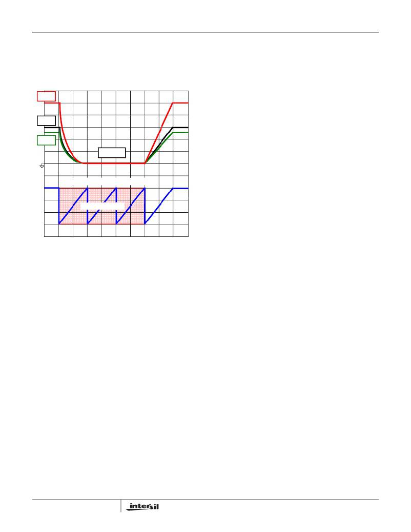
�V� DDQ�
�V� AGP�
�V� TT�
�500mV/DIV�
�INTERNAL SOFT-START FUNCTION�
�DELAY INTERVAL�
�V� TT� Over� Current� Protection�
�The� internal� V� TT� LDO� is� protected� from� fault� conditions�
�through� a� 3.3A� current� limit.� This� current� limit� protects� the�
�ISL6532C� if� the� LDO� is� sinking� or� sourcing� current.� During�
�an� overcurrent� event� on� the� V� TT� LDO,� only� the� V� TT� LDO� is�
�disabled.� Once� the� over� current� condition� on� the� V� TT� rail� is�
�removed,� V� TT� will� recover.�
�Over/Under� Voltage� Protection�
�All� three� regulators� are� protected� from� faults� through� internal�
�Over/Under� voltage� detection� circuitry.� If� the� any� rail� falls�
�below� 85%� of� the� targeted� voltage,� then� an� undervoltage�
�event� is� tripped.� An� under� voltage� will� disable� all� three�
�regulators� for� a� period� of� 3� soft-start� cycles,� after� which� a�
�normal� soft-start� is� initiated.� If� the� output� is� still� under� 85%� of�
�target,� the� regulators� will� continue� to� be� disabled� and� soft-�
�started� in� a� hiccup� mode� until� the� fault� is� cleared.� This�
�protection� feature� works� much� the� same� as� the� VDDQ� PWM�
�over� current� protection� works.� See� Figure� 3.�
�If� the� any� rail� exceeds� 115%� of� the� targeted� voltage,� then� all�
�three� outputs� are� immediately� disabled.� The� ISL6532C� will�
�not� re-enable� the� outputs� until� either� the� bias� voltage� is�
�toggled� in� order� to� initiate� a� POR� or� the� S5� signal� is� forced�
�LOW� and� then� back� to� HIGH.�
�T0�
�TIME�
�T1�
�T2�
�Thermal� Protection� (S0/S3� State)�
�I� PEAK� =� -----------------------------------------------------�
�I� PEAK� >� I� OUT� (� MAX� )� +� ----------� ,� where� ?� I� is�
�FIGURE� 3.� V� DDQ� and� V� TT� OVER� CURRENT� PROTECTION�
�AND� V� TT� /V� AGP� LDO� UNDER� VOLTAGE�
�PROTECTION� RESPONSES�
�The� over-current� function� will� trip� at� a� peak� inductor� current�
�(I� PEAK)� determined� by:�
�I� OCSET� x� R� OCSET�
�r� DS� (� ON� )�
�where� I� OCSET� is� the� internal� OCSET� current� source� (20� μ� A�
�typical).� The� OC� trip� point� varies� mainly� due� to� the� MOSFET�
�r� DS(ON)� variations.� To� avoid� over-current� tripping� in� the�
�normal� operating� load� range,� find� the� R� OCSET� resistor� from�
�the� equation� above� with:�
�1.� The� maximum� r� DS(ON)� at� the� highest� junction�
�temperature.�
�2.� The� minimum� I� OCSET� from� the� specification� table.�
�3.� Determine� I� PEAK� for:�
�(� ?� I� )�
�2�
�the� output� inductor� ripple� current.�
�For� an� equation� for� the� ripple� current� see� the� section� under�
�component� guidelines� titled� ‘Output� Inductor� Selection’.�
�A� small� ceramic� capacitor� should� be� placed� in� parallel� with�
�R� OCSET� to� smooth� the� voltage� across� R� OCSET� in� the�
�presence� of� switching� noise� on� the� input� voltage.�
�If� the� ISL6532C� IC� junction� temperature� reaches� a� nominal�
�temperature� of� 140� o� C,� all� regulators� will� be� disabled.� The�
�ISL6532C� will� not� re-enable� the� outputs� until� the� junction�
�temperature� drops� below� 110� o� C� and� either� the� bias� voltage�
�is� toggled� in� order� to� initiate� a� POR� or� the� SLP_S5� signal� is�
�forced� LOW� and� then� back� to� HIGH.�
�Shoot-Through� Protection�
�A� shoot-through� condition� occurs� when� both� the� upper� and�
�lower� MOSFETs� are� turned� on� simultaneously,� effectively�
�shorting� the� input� voltage� to� ground.� To� protect� from� a� shoot-�
�through� condition,� the� ISL6532C� incorporates� specialized�
�circuitry� which� insures� that� complementary� MOSFETs� are�
�not� ON� simultaneously.�
�The� adaptive� shoot-through� protection� utilized� by� the� V� DDQ�
�regulator� looks� at� the� lower� gate� drive� pin,� LGATE,� and� the�
�upper� gate� drive� pin,� UGATE,� to� determine� whether� a�
�MOSFET� is� ON� or� OFF.� If� the� voltage� from� UGATE� or� from�
�LGATE� to� GND� is� less� than� 0.8V,� then� the� respective�
�MOSFET� is� defined� as� being� OFF� and� the� other� MOSFET� is�
�allowed� to� turned� ON.� This� method� allows� the� V� DDQ�
�regulator� to� both� source� and� sink� current.�
�Since� the� voltage� of� the� MOSFET� gates� are� being� measured�
�to� determine� the� state� of� the� MOSFET,� the� designer� is�
�encouraged� to� consider� the� repercussions� of� introducing�
�external� components� between� the� gate� drivers� and� their�
�respective� MOSFET� gates� before� actually� implementing�
�such� measures.� Doing� so� may� interfere� with� the� shoot-�
�through� protection.�
�10�
�相关PDF资料 |
PDF描述 |
|---|---|
| RCC10DRXI-S734 | CONN EDGECARD 20POS DIP .100 SLD |
| GCC22DRES-S13 | CONN EDGECARD 44POS .100 EXTEND |
| GEC18DRXN-S734 | CONN EDGECARD 36POS DIP .100 SLD |
| RCE05DHHN | CONN EDGECARD 10POS DIP 1MM SLD |
| EVAL-ADCMP552BRQZ | BOARD EVALUATION ADCMP552BRQZ |
相关代理商/技术参数 |
参数描述 |
|---|---|
| ISL6532CCR-T | 功能描述:IC REG/CTRLR ACPI DUAL DDR 28QFN RoHS:否 类别:集成电路 (IC) >> PMIC - 电源管理 - 专用 系列:- 应用说明:Ultrasound Imaging Systems Application Note 产品培训模块:Lead (SnPb) Finish for COTS Obsolescence Mitigation Program 标准包装:37 系列:- 应用:医疗用超声波成像,声纳 电流 - 电源:- 电源电压:2.37 V ~ 6 V 工作温度:0°C ~ 70°C 安装类型:表面贴装 封装/外壳:56-WFQFN 裸露焊盘 供应商设备封装:56-TQFN-EP(8x8) 包装:管件 |
| ISL6532CCRZ | 功能描述:IC REG/CTRLR ACPI DUAL DDR 28QFN RoHS:是 类别:集成电路 (IC) >> PMIC - 电源管理 - 专用 系列:- 应用说明:Ultrasound Imaging Systems Application Note 产品培训模块:Lead (SnPb) Finish for COTS Obsolescence Mitigation Program 标准包装:37 系列:- 应用:医疗用超声波成像,声纳 电流 - 电源:- 电源电压:2.37 V ~ 6 V 工作温度:0°C ~ 70°C 安装类型:表面贴装 封装/外壳:56-WFQFN 裸露焊盘 供应商设备封装:56-TQFN-EP(8x8) 包装:管件 |
| ISL6532CCRZ-T | 功能描述:IC REG/CTRLR ACPI DUAL DDR 28QFN RoHS:是 类别:集成电路 (IC) >> PMIC - 电源管理 - 专用 系列:- 应用说明:Ultrasound Imaging Systems Application Note 产品培训模块:Lead (SnPb) Finish for COTS Obsolescence Mitigation Program 标准包装:37 系列:- 应用:医疗用超声波成像,声纳 电流 - 电源:- 电源电压:2.37 V ~ 6 V 工作温度:0°C ~ 70°C 安装类型:表面贴装 封装/外壳:56-WFQFN 裸露焊盘 供应商设备封装:56-TQFN-EP(8x8) 包装:管件 |
| ISL6532CR | 功能描述:IC REG/CTRLR ACPI DUAL DDR 20QFN RoHS:否 类别:集成电路 (IC) >> PMIC - 电源管理 - 专用 系列:- 应用说明:Ultrasound Imaging Systems Application Note 产品培训模块:Lead (SnPb) Finish for COTS Obsolescence Mitigation Program 标准包装:37 系列:- 应用:医疗用超声波成像,声纳 电流 - 电源:- 电源电压:2.37 V ~ 6 V 工作温度:0°C ~ 70°C 安装类型:表面贴装 封装/外壳:56-WFQFN 裸露焊盘 供应商设备封装:56-TQFN-EP(8x8) 包装:管件 |
| ISL6532CR-T | 功能描述:IC REG/CTRLR ACPI DUAL DDR 20QFN RoHS:否 类别:集成电路 (IC) >> PMIC - 电源管理 - 专用 系列:- 应用说明:Ultrasound Imaging Systems Application Note 产品培训模块:Lead (SnPb) Finish for COTS Obsolescence Mitigation Program 标准包装:37 系列:- 应用:医疗用超声波成像,声纳 电流 - 电源:- 电源电压:2.37 V ~ 6 V 工作温度:0°C ~ 70°C 安装类型:表面贴装 封装/外壳:56-WFQFN 裸露焊盘 供应商设备封装:56-TQFN-EP(8x8) 包装:管件 |
发布紧急采购,3分钟左右您将得到回复。