- 您现在的位置:买卖IC网 > PDF目录16597 > ISL6532CCR (Intersil)IC REG/CTRLR ACPI DUAL DDR 28QFN PDF资料下载
参数资料
| 型号: | ISL6532CCR |
| 厂商: | Intersil |
| 文件页数: | 9/16页 |
| 文件大小: | 0K |
| 描述: | IC REG/CTRLR ACPI DUAL DDR 28QFN |
| 标准包装: | 50 |
| 应用: | 存储器,DDR/DDR2 稳压器 |
| 电流 - 电源: | 5.25mA |
| 工作温度: | 0°C ~ 70°C |
| 安装类型: | 表面贴装 |
| 封装/外壳: | 28-VQFN 裸露焊盘 |
| 供应商设备封装: | 28-QFN(6x6) |
| 包装: | 管件 |
�� �
�
�ISL6532C�
�Figure� 1� shows� the� soft� start� sequence� for� a� typical� cold�
�start.� Due� to� the� soft� start� capacitance,� C� SS� ,� on� the�
�VREF_IN� pin,� the� S5� to� S0� transition� profile� of� the� V� TT� rail�
�will� have� a� more� rounded� features� at� the� start� and� end� of� the�
�soft� start� whereas� the� V� DDQ� profile� has� distinct� starting� and�
�S3�
�S5�
�12VATX� 2V/DIV�
�ending� points� to� the� ramp� up.�
�By� directly� monitoring� 12VATX� and� the� SLP_S3� and� SLP_S5�
�signals� the� ISL6532C� can� achieve� PGOOD� status�
�V� AGP�
�500mV/DIV�
�V� DDQ�
�500mV/DIV�
�significantly� faster� than� other� devices� that� depend� on�
�Latched_Backfeed_Cut� for� timing.�
�V� TT_FLOAT�
�V� TT�
�500mV/DIV�
�Active� to� Sleep� (S0� to� S3� Transition)�
�When� SLP_S3� goes� LOW� with� SLP_S5� still� HIGH,� the�
�ISL6532C� will� disable� the� V� TT� linear� regulator� and� the� AGP�
�LDO� controller.� The� V� DDQ� standby� regulator� will� be� enabled�
�and� the� V� DDQ� switching� regulator� will� be� disabled.� NCH� is�
�pulled� low� to� disable� the� backfeed� blocking� MOSFET.�
�PGOOD� will� also� transition� LOW.� When� V� TT� is� disabled,� the�
�internal� reference� for� the� V� TT� regulator� is� internally� shorted�
�to� the� V� TT� rail.� This� allows� the� V� TT� rail� to� float.� When�
�floating,� the� voltage� on� the� V� TT� rail� will� depend� on� the�
�leakage� characteristics� of� the� memory� and� MCH� I/O� pins.� It�
�is� important� to� note� that� the� V� TT� rail� may� not� bleed� down� to� 0V.�
�The� V� DDQ� rail� will� be� supported� in� the� S3� state� through� the�
�standby� V� DDQ� LDO.� When� S3� transitions� LOW,� the� Standby�
�regulator� is� immediately� enabled.� The� switching� regulator� is�
�disabled� synchronous� to� the� switching� waveform.� The� shut�
�off� time� will� range� between� 4� and� 8� μ� s.� The� standby� LDO� is�
�capable� of� supporting� up� to� 650mA� of� load� with� P5VSBY� tied�
�to� the� 5V� Standby� Rail.� The� standby� LDO� may� receive� input�
�from� either� the� 3.3V� Standby� rail� or� the� 5V� Standby� rail�
�through� the� P5VSBY� pin.� It� is� recommended� that� the� 5V�
�Standby� rail� be� used� as� the� current� delivery� capability� of� the�
�LDO� is� greater.�
�Sleep� to� Active� (S3� to� S0� Transition)�
�When� SLP_S3� transitions� from� LOW� to� HIGH� with� SLP_S5�
�held� HIGH� and� after� the� 12V� rail� exceeds� POR,� the�
�ISL6532C� will� enable� the� V� DDQ� switching� regulator,� disable�
�the� V� DDQ� standby� regulator,� enable� the� V� TT� LDO� and� force�
�the� NCH� pin� to� a� high� impedance� state� turning� on� the�
�blocking� MOSFET.� The� AGP� LDO� goes� through� a� 2048� clock�
�cycle� soft-start.� The� internal� short� between� the� V� TT�
�reference� and� the� V� TT� rail� is� released.� Upon� release� of� the�
�short,� the� capacitor� on� VREF_IN� is� then� charged� up� through�
�the� internal� resistor� divider� network.� The� V� TT� output� will�
�follow� this� capacitor� charge� up,� and� acting� as� the� S3� to� S0�
�transition� soft� start� for� the� V� TT� rail.� The� PGOOD� comparator�
�is� enabled� only� after� 2048� clock� cycles,� or� typically� 8.2ms,�
�have� passed� following� the� S3� transition� to� a� HIGH� state.�
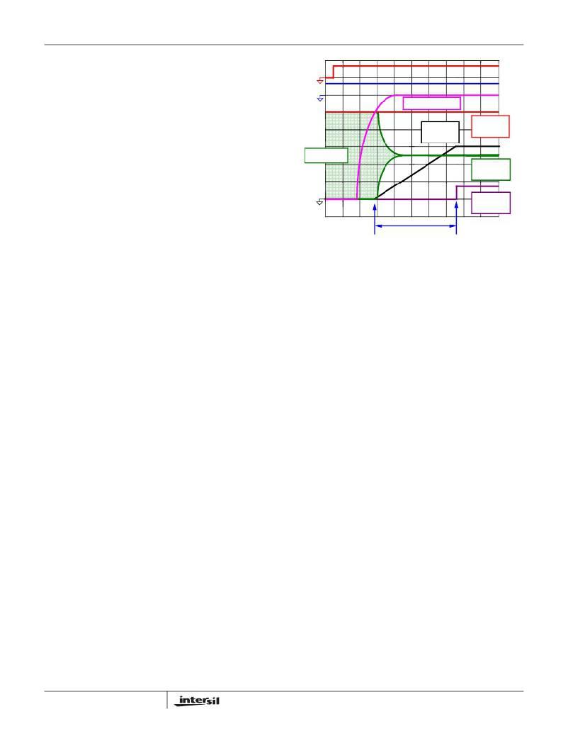
�Figure� 2� illustrates� a� typical� state� transition� from� S3� to� S0.� It�
�should� be� noted� that� the� soft� start� profile� of� the� V� TT� LDO�
�output� will� vary� according� to� the� value� of� the� capacitor� on� the�
�VREF_IN� pin.�
�PGOOD�
�5V/DIV�
�2048� CLOCK�
�CYCLES�
�12V� POR� PGOOD� COMPARATOR�
�ENABLED�
�FIGURE� 2.� TYPICAL� S3� TO� S0� STATE� TRANSITION�
�Active� to� Shutdown� (S0� to� S5� Transition)�
�When� the� system� transitions� from� active,� S0,� state� to�
�shutdown,� S4/S5,� state,� the� ISL6532C� IC� disables� all�
�regulators� and� forces� the� PGOOD� pin� and� the� NCH� pin� LOW.�
�V� DDQ� Over� Current� Protection� (S0� State)�
�The� over-current� function� protects� the� switching� converter�
�from� a� shorted� output� by� using� the� upper� MOSFET� on-�
�resistance,� r� DS(ON)� ,� to� monitor� the� current.� This� method�
�enhances� the� converter’s� efficiency� and� reduces� cost� by�
�eliminating� a� current� sensing� resistor.�
�The� over-current� function� cycles� the� soft-start� function� in� a�
�hiccup� mode� to� provide� fault� protection.� A� resistor� (R� OCSET� )�
�programs� the� over-current� trip� level� (see� Typical� Application�
�diagrams� on� pages� 3� and� 4).� An� internal� 20� μ� A� (typical)�
�current� sink� develops� a� voltage� across� R� OCSET� that� is�
�referenced� to� the� converter� input� voltage.� When� the� voltage�
�across� the� upper� MOSFET� (also� referenced� to� the� converter�
�input� voltage)� exceeds� the� voltage� across� R� OCSET� ,� the� over-�
�current� function� initiates� a� soft-start� sequence.� The� initiation�
�of� soft� start� will� affect� all� regulators.� The� V� TT� regulator� is�
�directly� affected� as� it� receives� it’s� reference� from� V� DDQ� .� The�
�AGP� LDO� will� also� be� soft� started,� and� as� such,� the� AGP�
�LDO� voltage� will� be� disabled� while� the� V� DDQ� regulator� is�
�disabled.�
�Figure� 3� illustrates� the� protection� feature� responding� to� an�
�over� current� event.� At� time� T0,� an� over� current� condition� is�
�sensed� across� the� upper� MOSFET.� As� a� result,� the� regulator�
�is� quickly� shutdown� and� the� internal� soft-start� function�
�begins� producing� soft-start� ramps.� The� delay� interval� seen�
�by� the� output� is� equivalent� to� three� soft-start� cycles.� The�
�fourth� internal� soft-start� cycle� initiates� a� normal� soft-start�
�ramp� of� the� output,� at� time� T1.� The� output� is� brought� back�
�into� regulation� by� time� T2,� as� long� as� the� over� current� event�
�has� cleared.�
�9�
�相关PDF资料 |
PDF描述 |
|---|---|
| RCC10DRXI-S734 | CONN EDGECARD 20POS DIP .100 SLD |
| GCC22DRES-S13 | CONN EDGECARD 44POS .100 EXTEND |
| GEC18DRXN-S734 | CONN EDGECARD 36POS DIP .100 SLD |
| RCE05DHHN | CONN EDGECARD 10POS DIP 1MM SLD |
| EVAL-ADCMP552BRQZ | BOARD EVALUATION ADCMP552BRQZ |
相关代理商/技术参数 |
参数描述 |
|---|---|
| ISL6532CCR-T | 功能描述:IC REG/CTRLR ACPI DUAL DDR 28QFN RoHS:否 类别:集成电路 (IC) >> PMIC - 电源管理 - 专用 系列:- 应用说明:Ultrasound Imaging Systems Application Note 产品培训模块:Lead (SnPb) Finish for COTS Obsolescence Mitigation Program 标准包装:37 系列:- 应用:医疗用超声波成像,声纳 电流 - 电源:- 电源电压:2.37 V ~ 6 V 工作温度:0°C ~ 70°C 安装类型:表面贴装 封装/外壳:56-WFQFN 裸露焊盘 供应商设备封装:56-TQFN-EP(8x8) 包装:管件 |
| ISL6532CCRZ | 功能描述:IC REG/CTRLR ACPI DUAL DDR 28QFN RoHS:是 类别:集成电路 (IC) >> PMIC - 电源管理 - 专用 系列:- 应用说明:Ultrasound Imaging Systems Application Note 产品培训模块:Lead (SnPb) Finish for COTS Obsolescence Mitigation Program 标准包装:37 系列:- 应用:医疗用超声波成像,声纳 电流 - 电源:- 电源电压:2.37 V ~ 6 V 工作温度:0°C ~ 70°C 安装类型:表面贴装 封装/外壳:56-WFQFN 裸露焊盘 供应商设备封装:56-TQFN-EP(8x8) 包装:管件 |
| ISL6532CCRZ-T | 功能描述:IC REG/CTRLR ACPI DUAL DDR 28QFN RoHS:是 类别:集成电路 (IC) >> PMIC - 电源管理 - 专用 系列:- 应用说明:Ultrasound Imaging Systems Application Note 产品培训模块:Lead (SnPb) Finish for COTS Obsolescence Mitigation Program 标准包装:37 系列:- 应用:医疗用超声波成像,声纳 电流 - 电源:- 电源电压:2.37 V ~ 6 V 工作温度:0°C ~ 70°C 安装类型:表面贴装 封装/外壳:56-WFQFN 裸露焊盘 供应商设备封装:56-TQFN-EP(8x8) 包装:管件 |
| ISL6532CR | 功能描述:IC REG/CTRLR ACPI DUAL DDR 20QFN RoHS:否 类别:集成电路 (IC) >> PMIC - 电源管理 - 专用 系列:- 应用说明:Ultrasound Imaging Systems Application Note 产品培训模块:Lead (SnPb) Finish for COTS Obsolescence Mitigation Program 标准包装:37 系列:- 应用:医疗用超声波成像,声纳 电流 - 电源:- 电源电压:2.37 V ~ 6 V 工作温度:0°C ~ 70°C 安装类型:表面贴装 封装/外壳:56-WFQFN 裸露焊盘 供应商设备封装:56-TQFN-EP(8x8) 包装:管件 |
| ISL6532CR-T | 功能描述:IC REG/CTRLR ACPI DUAL DDR 20QFN RoHS:否 类别:集成电路 (IC) >> PMIC - 电源管理 - 专用 系列:- 应用说明:Ultrasound Imaging Systems Application Note 产品培训模块:Lead (SnPb) Finish for COTS Obsolescence Mitigation Program 标准包装:37 系列:- 应用:医疗用超声波成像,声纳 电流 - 电源:- 电源电压:2.37 V ~ 6 V 工作温度:0°C ~ 70°C 安装类型:表面贴装 封装/外壳:56-WFQFN 裸露焊盘 供应商设备封装:56-TQFN-EP(8x8) 包装:管件 |
发布紧急采购,3分钟左右您将得到回复。