参数资料
| 型号: | ISL65426HRZ |
| 厂商: | Intersil |
| 文件页数: | 15/22页 |
| 文件大小: | 0K |
| 描述: | IC REG BUCK SYNC ADJ 6A DL 50QFN |
| 产品培训模块: | Dual Synchronous Integrated FET Buck Regulator Solutions for Industrial Control Applications |
| 标准包装: | 30 |
| 类型: | 降压(降压) |
| 输出类型: | 可调式 |
| 输出数: | 2 |
| 输出电压: | 1 V ~ 4 V |
| 输入电压: | 3 V ~ 5.5 V |
| PWM 型: | 电流模式 |
| 频率 - 开关: | 1MHz |
| 电流 - 输出: | 6A |
| 同步整流器: | 是 |
| 工作温度: | -10°C ~ 100°C |
| 安装类型: | 表面贴装 |
| 封装/外壳: | 50-VFQFN 裸露焊盘 |
| 包装: | 管件 |
| 供应商设备封装: | 50-QFN(5x10) |
| 产品目录页面: | 1248 (CN2011-ZH PDF) |
�� �
�
�ISL65426�
�EN�
�System� enable� for� voltage� monitoring� with� programmable�
�hysteresis.� This� pin� has� a� POR� rising� threshold� of� 0.6V.� This�
�enable� is� intended� for� applications� where� two� or� more� input�
�power� supplies� are� used� and� bias� rise� time� is� an� issue.�
�The� remaining� four� floating� power� blocks� can� be� partitioned�
�in� one� of� four� valid� states� outlined� in� Table� 1.� The� controller�
�detects� the� programmed� configuration� based� on� the� state� of�
�logic� signals� at� pins� ISET1� and� ISET2.� The� controller� checks�
�the� power� block� configuration� versus� the� programmed�
�configuration� before� the� either� converter� can� soft-start.�
�EN1,� EN2�
�These� pins� are� threshold-sensitive� enable� inputs� for� the�
�individual� PWM� converters.� These� pins� have� low� current�
�(10μA)� internal� pull-ups� to� VCC.� This� pin� disables� the�
�respective� converter� until� pulled� above� a� 1V� rising� threshold.�
�ISET1,� ISET2�
�Power� block� configuration� inputs.� Select� the� proper� state� for�
�Each� power� block� has� a� separate� power� supply� connection�
�pin,� PVINx,� and� common� channels� must� join� these� inputs� to�
�one� input� power� supply.� Common� synchronous� power� switch�
�connection� points� for� each� channel� must� be� tied� together�
�and� to� an� external� inductor.� See� the� “Typical� Application�
�Schematics”� for� pin� connection� guidance.�
�TABLE� 1.� POWER� BLOCK� CONFIGURATION�
�each� pin� according� to� Table� 1.�
�V1SET1,� V1SET2,� V2SET1,� V2SET2�
�CHANNEL� 1�
�ISET1� ISET2� I� OUT1� CONNECTIONS� I� OUT2�
�CHANNEL� 2�
�CONNECTIONS�
�Output� voltage� configuration� inputs.� Select� the� proper� state�
�of� each� pin� per� the� “Electrical� Specifications”� table.�
�PG1,� PG2�
�1�
�1�
�0�
�1�
�0�
�1�
�3A�
�4A�
�5A�
�LX1,LX2,LX3�
�LX1,LX2,LX3,LX4�
�LX1,LX2,LX3,�
�3A�
�2A�
�1A�
�LX4,LX5,LX6�
�LX5,LX6�
�LX5�
�Power-good� output.� Open� drain� logic� output� that� is� pulled� to�
�LX4,LX6�
�ground� when� the� output� voltage� is� outside� regulation� limits.�
�0�
�0�
�2A�
�LX1,LX2�
�4A�
�LX3,LX4,LX5,LX6�
�Functional� Description�
�Invalid� LX� Configurations:� SS� Prevented�
�The� ISL65426� is� a� monolithic,� constant� frequency,� current-�
�mode� dual� output� buck� converter� controller� with� user�
�X�
�X�
�1A�
�LX2�
�5A�
�LX1,LX3,LX4,�
�LX5,LX6�
�configurable� power� blocks.� Designed� to� provide� a� total�
�DC/DC� solution� for� FPGAs,� CPLDs,� core� processors,� and�
�ASICs.�
�Each� power� block� has� a� scaled� pilot� device� providing� current�
�feedback.� The� configuration� pin� settling� determines� how� the�
�controller� handles� separation� and� summing� of� the� individual�
�current� feedback� signals.�
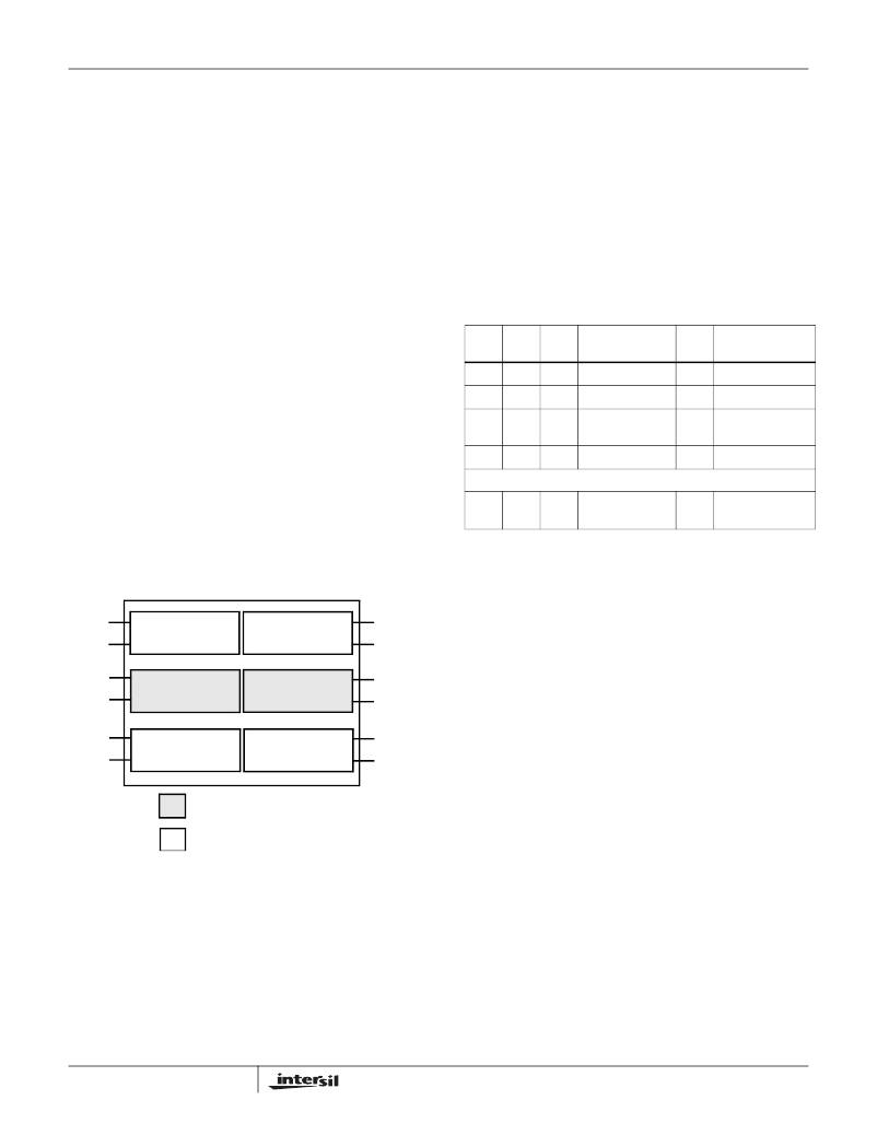
�PVIN1�
�LX1�
�PVIN2�
�LX2�
�POWER� BLOCK� 1�
�POWER� BLOCK� 2�
�POWER� BLOCK� 6�
�POWER� BLOCK� 5�
�PVIN6�
�LX6�
�PVIN5�
�LX5�
�Main� Control� Loop�
�The� ISL65426� is� a� monolithic,� constant� frequency,�
�current� mode� step-down� DC/DC� converter.� During� normal�
�operation,� the� internal� top� power� switch� is� turned� on� at� the�
�beginning� of� each� clock� cycle.� Current� in� the� output� inductor�
�ramps� up� until� the� current� comparator� trips� and� turns� off� the�
�PVIN3�
�LX3�
�POWER� BLOCK� 3�
�POWER� BLOCK� 4�
�PVIN4�
�LX4�
�top� power� MOSFET.� The� bottom� power� MOSFET� turns� on�
�and� the� inductor� current� ramps� down� for� the� rest� of� the� cycle.�
�The� current� comparator� compares� the� output� current� at� the�
�MASTER� POWER� BLOCK�
�FLOATING� POWER� BLOCK�
�FIGURE� 35.� POWER� BLOCK� DIAGRAM�
�Power� Blocks�
�A� unique� power� block� architecture� allows� partitioning� of� six�
�1A� capable� modules� to� support� one� of� four� power� block�
�configuration� options.� The� block� diagram� in� Figure� 3�
�provides� a� top� level� view� of� the� power� block� layout.� One�
�master� power� block� is� assigned� to� each� converter� output�
�channel.� Power� Block� 2� is� allotted� to� converter� Channel� 1�
�and� Power� Block� 5� to� Channel� 2.� The� master� power� blocks�
�must� not� be� tied� together� or� the� controller� will� not� soft-start.�
�15�
�ripple� current� peak� to� a� current� pilot.� The� error� amplifier�
�monitors� V� OUT� and� compares� it� with� the� internal� voltage�
�reference.� The� error� amplifier� ’s� output� voltage� drives� a�
�proportional� current� to� the� pilot.� If� V� OUT� is� low� the� pilot’s�
�current� level� is� increased� and� the� trip� off� current� level� of� the�
�output� is� increased.� The� increased� current� works� to� raise� the�
�V� OUT� level� into� agreement� with� the� voltage� reference.�
�Output� Voltage� Programming�
�The� feedback� voltage� applied� to� the� inverting� input� of� the�
�error� amplifier� is� scaled� internally� relative� to� the� 0.6V� internal�
�reference� voltage� based� on� the� state� of� logic� signals� at� pins�
�V1SET1,� V1SET2,� V2SET1� and� V2SET2.� The� output�
�voltage� configuration� logic� decodes� the� 2-bit� voltage�
�identification� codes� into� one� of� the� discrete� voltages� shown�
�FN6340.3�
�March� 25,� 2008�
�相关PDF资料 |
PDF描述 |
|---|---|
| ISL6545IBZ-T | IC REG CTRLR BUCK PWM VM 8-SOIC |
| ISL6548ACRZA-T | IC REG/CTLR ACPI DUAL DDR 28QFN |
| ISL6548CRZA | IC REG/CTRLR ACPI DUAL DDR 28QFN |
| ISL6551IR-T | IC REG CTRLR FLYBACK PWM 28-QFN |
| ISL6552CR-T | IC REG CTRLR BUCK PWM 20-QFN |
相关代理商/技术参数 |
参数描述 |
|---|---|
| ISL65426HRZS2698 | 制造商:Intersil Corporation 功能描述:LEAD-FREE W/ANNEAL, DUAL BUCK REGULATOR. -10 TO +100 TEMP. - Rail/Tube 制造商:Intersil 功能描述:W/ANNEAL DL BUCKG -10 TO +100 TEMP |
| ISL65426HRZS2715 | 制造商:Intersil Corporation 功能描述:S SPEC FOR TRACKING BROADCOM BUSINESS ONLY-SOLD THRU DISTI - Rail/Tube |
| ISL65426HRZ-T | 功能描述:IC REG BUCK SYNC ADJ 6A DL 50QFN RoHS:是 类别:集成电路 (IC) >> PMIC - 稳压器 - DC DC 开关稳压器 系列:- 产品培训模块:Lead (SnPb) Finish for COTS Obsolescence Mitigation Program 标准包装:2,500 系列:- 类型:降压(降压) 输出类型:两者兼有 输出数:1 输出电压:5V,1 V ~ 10 V 输入电压:3.5 V ~ 28 V PWM 型:电流模式 频率 - 开关:220kHz ~ 1MHz 电流 - 输出:600mA 同步整流器:无 工作温度:-40°C ~ 125°C 安装类型:表面贴装 封装/外壳:16-SSOP(0.154",3.90mm 宽) 包装:带卷 (TR) 供应商设备封装:16-QSOP |
| ISL65426HRZ-TS2698 | 制造商:Intersil Corporation 功能描述:LEAD-FREE W/ANNEAL, DUAL BUCK REGULATOR. -10 TO +100 TEMP. - Tape and Reel 制造商:Intersil 功能描述:W/ANNEAL DL BUCKG -10 TO +100 TEMP |
| ISL65426HRZ-TS2715 | 制造商:Intersil Corporation 功能描述:S SPEC FOR TRACKING BROADCOM BUSINESS ONLY-SOLD THRU DISTI - Tape and Reel |
发布紧急采购,3分钟左右您将得到回复。