参数资料
| 型号: | ISL65426HRZ |
| 厂商: | Intersil |
| 文件页数: | 20/22页 |
| 文件大小: | 0K |
| 描述: | IC REG BUCK SYNC ADJ 6A DL 50QFN |
| 产品培训模块: | Dual Synchronous Integrated FET Buck Regulator Solutions for Industrial Control Applications |
| 标准包装: | 30 |
| 类型: | 降压(降压) |
| 输出类型: | 可调式 |
| 输出数: | 2 |
| 输出电压: | 1 V ~ 4 V |
| 输入电压: | 3 V ~ 5.5 V |
| PWM 型: | 电流模式 |
| 频率 - 开关: | 1MHz |
| 电流 - 输出: | 6A |
| 同步整流器: | 是 |
| 工作温度: | -10°C ~ 100°C |
| 安装类型: | 表面贴装 |
| 封装/外壳: | 50-VFQFN 裸露焊盘 |
| 包装: | 管件 |
| 供应商设备封装: | 50-QFN(5x10) |
| 产品目录页面: | 1248 (CN2011-ZH PDF) |
�� �
�
�ISL65426�
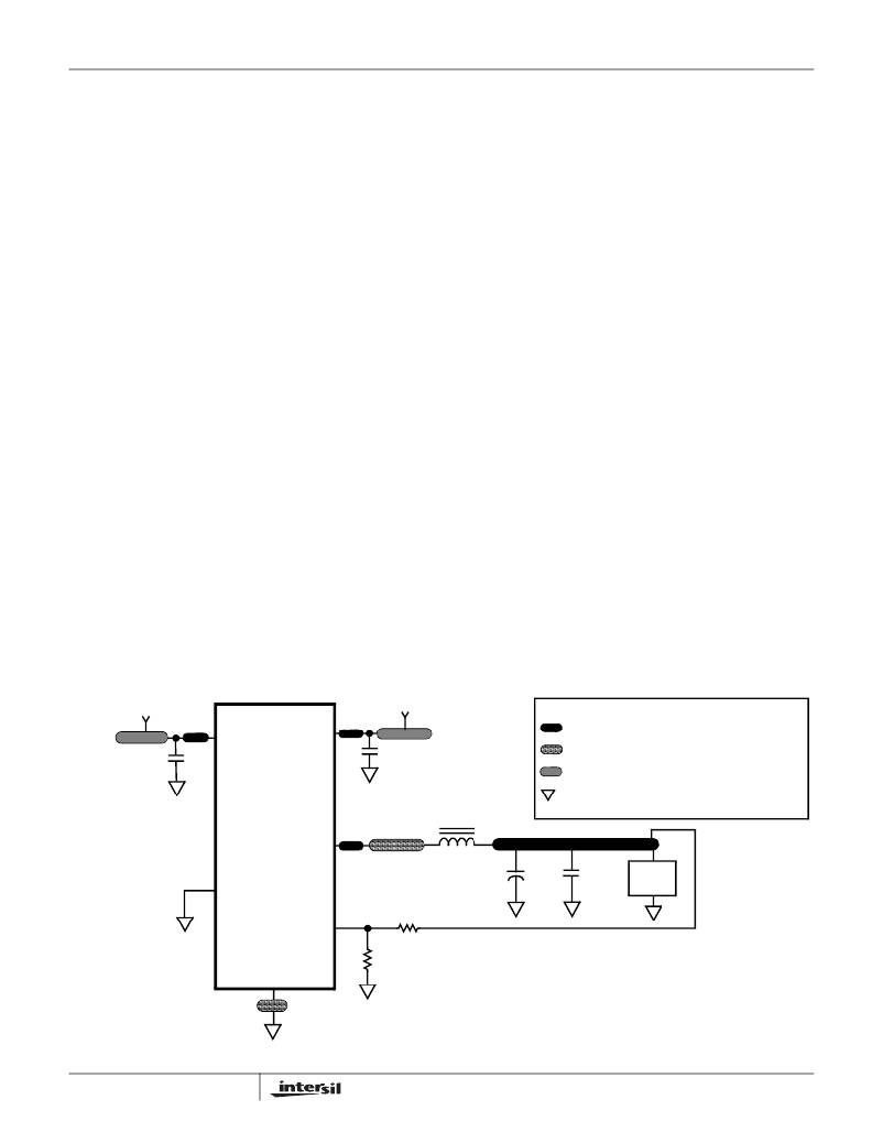
�The� following� multi-layer� printed� circuitry� board� layout�
�strategies� minimize� the� impact� of� board� parasitics� on�
�converter� performance� and� optimize� the� heat-dissipating�
�capabilities� of� the� printed� circuit� board.� This� section�
�highlights� some� important� practices� which� should� not� be�
�overlooked� during� the� layout� process.� Figure� 38� provides� a�
�top� level� view� of� the� critical� components,� layer� utilization,�
�and� signal� routing� for� reference.�
�Component� Placement�
�Determine� the� total� implementation� area� and� orient� the�
�critical� switching� components� first.� These� include� the�
�controller,� input� and� output� capacitors,� and� the� output�
�inductors.� Symmetry� is� very� important� in� determining� how�
�available� space� is� filled� and� depends� on� the� power� block�
�configuration� selected.� The� controller� must� be� placed�
�equidistant� from� each� output� stage� with� the� LX� or� phase�
�connection� distance� minimized.�
�An� output� stage� consists� of� the� area� reserved� for� the� output�
�inductor,� and� input� capacitors,� and� output� capacitors� for� a�
�single� channel.� Place� the� inductor� such� that� one� pad� is� a�
�minimal� distance� from� the� associated� phase� connection.�
�Orient� the� inductor� such� that� the� load� device� is� a� short�
�distance� from� the� other� pad.� Placing� the� input� capacitors� a�
�minimal� distance� from� the� PVIN� pins� prevents� long� distances�
�from� adding� too� much� trace� inductance� and� a� reduction� in�
�capacitor� performance.� Locate� the� output� capacitors�
�between� the� inductor� and� the� load� device,� while� keeping�
�them� in� close� proximity.� Care� should� be� taken� not� to� add�
�inductance� through� long� trace� lengths� that� could� cancel� the�
�usefulness� of� the� low� inductance� components.� Keeping� the�
�components� in� tight� proximity� will� help� reduce� parasitic�
�impedances� once� the� components� are� routed� together.�
�Bypass� capacitors,� C� BP� ,� supply� critical� filtering� and� must� be�
�placed� close� to� their� respective� pins.� Stray� trace� parasitics�
�will� reduce� their� effectiveness,� so� keep� the� distance� between�
�the� VCC� bias� supply� pad� and� capacitor� pad� to� a� minimum.�
�Plane� Allocation�
�PCB� designers� typically� have� a� set� number� of� planes�
�available� for� a� converter� design.� Dedicate� one� solid� layer,�
�(usually� an� internal� layer� underneath� the� component� side� of�
�the� board),� for� a� ground� plane� and� make� all� critical�
�component� ground� connections� with� vias� to� this� layer.�
�One� additional� solid� layer� is� dedicated� as� a� power� plane� and�
�broken� into� smaller� islands� of� common� voltage.� The� power�
�plane� should� support� the� input� power� and� output� power�
�nodes.� Use� copper� filled� polygons� on� the� top� and� bottom�
�circuit� layers� for� the� phase� nodes.� Use� the� remaining� printed�
�circuit� board� layers� for� small� signal� wiring� and� additional�
�power� or� ground� islands� as� required.�
�Signal� Routing�
�If� the� output� stage� component� placement� guidelines� are�
�followed,� stray� inductance� in� the� switch� current� path� is�
�minimized� along� with� good� routing� techniques.� Great�
�attention� should� be� paid� to� routing� the� PHASE� plane� since�
�high� current� pulses� are� driven� through� them.� Stray�
�inductance� in� this� high-current� path� induces� large� noise�
�voltages� that� couple� into� sensitive� circuitry.� By� keeping� the�
�PHASE� plane� small,� the� magnitude� of� the� potential� spikes� is�
�minimized.� It� is� important� to� size� traces� from� the� LX� pins� to�
�the� PHASE� plane� as� large� and� short� as� possible� to� reduce�
�their� overall� impedance� and� inductance.�
�V� IN�
�C� BP�
�VCC�
�PVIN�
�V� IN�
�C� IN�
�KEY�
�THICK� TRACE� ON� CIRCUIT� PLANE� LAYER�
�ISLAND� ON� CIRCUIT� PLANE� LAYER�
�ISLAND� ON� POWER� PLANE� LAYER�
�VIA� CONNECTION� TO� GROUND� PLANE�
�ISL65426�
�LX�
�PHASE�
�L� OUT�
�V� OUT�
�C� OUT�
�C� HFOUT�
�LOAD�
�GND�
�FB�
�PGND�
�FIGURE� 38.� PRINTED� CIRCUIT� BOARD� POWER� PLANES� AND� ISLANDS�
�20�
�FN6340.3�
�March� 25,� 2008�
�相关PDF资料 |
PDF描述 |
|---|---|
| ISL6545IBZ-T | IC REG CTRLR BUCK PWM VM 8-SOIC |
| ISL6548ACRZA-T | IC REG/CTLR ACPI DUAL DDR 28QFN |
| ISL6548CRZA | IC REG/CTRLR ACPI DUAL DDR 28QFN |
| ISL6551IR-T | IC REG CTRLR FLYBACK PWM 28-QFN |
| ISL6552CR-T | IC REG CTRLR BUCK PWM 20-QFN |
相关代理商/技术参数 |
参数描述 |
|---|---|
| ISL65426HRZS2698 | 制造商:Intersil Corporation 功能描述:LEAD-FREE W/ANNEAL, DUAL BUCK REGULATOR. -10 TO +100 TEMP. - Rail/Tube 制造商:Intersil 功能描述:W/ANNEAL DL BUCKG -10 TO +100 TEMP |
| ISL65426HRZS2715 | 制造商:Intersil Corporation 功能描述:S SPEC FOR TRACKING BROADCOM BUSINESS ONLY-SOLD THRU DISTI - Rail/Tube |
| ISL65426HRZ-T | 功能描述:IC REG BUCK SYNC ADJ 6A DL 50QFN RoHS:是 类别:集成电路 (IC) >> PMIC - 稳压器 - DC DC 开关稳压器 系列:- 产品培训模块:Lead (SnPb) Finish for COTS Obsolescence Mitigation Program 标准包装:2,500 系列:- 类型:降压(降压) 输出类型:两者兼有 输出数:1 输出电压:5V,1 V ~ 10 V 输入电压:3.5 V ~ 28 V PWM 型:电流模式 频率 - 开关:220kHz ~ 1MHz 电流 - 输出:600mA 同步整流器:无 工作温度:-40°C ~ 125°C 安装类型:表面贴装 封装/外壳:16-SSOP(0.154",3.90mm 宽) 包装:带卷 (TR) 供应商设备封装:16-QSOP |
| ISL65426HRZ-TS2698 | 制造商:Intersil Corporation 功能描述:LEAD-FREE W/ANNEAL, DUAL BUCK REGULATOR. -10 TO +100 TEMP. - Tape and Reel 制造商:Intersil 功能描述:W/ANNEAL DL BUCKG -10 TO +100 TEMP |
| ISL65426HRZ-TS2715 | 制造商:Intersil Corporation 功能描述:S SPEC FOR TRACKING BROADCOM BUSINESS ONLY-SOLD THRU DISTI - Tape and Reel |
发布紧急采购,3分钟左右您将得到回复。