参数资料
| 型号: | ISL6551IR-T |
| 厂商: | Intersil |
| 文件页数: | 10/26页 |
| 文件大小: | 0K |
| 描述: | IC REG CTRLR FLYBACK PWM 28-QFN |
| 标准包装: | 4,000 |
| PWM 型: | 电流模式 |
| 输出数: | 6 |
| 频率 - 最大: | 1MHz |
| 占空比: | 50% |
| 电源电压: | 10.8 V ~ 13.2 V |
| 降压: | 无 |
| 升压: | 无 |
| 回扫: | 是 |
| 反相: | 无 |
| 倍增器: | 无 |
| 除法器: | 无 |
| Cuk: | 无 |
| 隔离: | 无 |
| 工作温度: | 0°C ~ 85°C |
| 封装/外壳: | 28-VQFN 裸露焊盘 |
| 包装: | 带卷 (TR) |
�� �
�
�ISL6551�
�Block/Pin� Functional� Descriptions�
�Detailed� descriptions� of� each� individual� block� in� the� functional�
�block� diagram� on� page� 3� are� included� in� this� section.�
�Application� information� and� design� considerations� for� each� pin�
�and/or� each� block� are� also� included.�
�?� IC� Bias� Power� (VDD,� VDDP1,� VDDP2)�
�-� The� IC� is� powered� from� a� 12V� ±� 10%� supply.�
�-� VDD� supplies� power� to� both� the� digital� and� analog� circuits�
�and� should� be� bypassed� directly� to� the� VSS� pin� with� an�
�0.1� μ� F� low� ESR� ceramic� capacitor.�
�-� VDDP1� and� VDDP2� are� the� bias� supplies� for� the� upper�
�drivers� and� the� lower� drivers,� respectively.� They� should� be�
�decoupled� with� ceramic� capacitors� to� the� PGND� pin.�
�-� Heavy� copper� should� be� attached� to� these� pins� for� a� better�
�heat� spreading.�
�?� IC� GNDs� (VSS,� PGND)�
�-� VSS� is� the� reference� ground,� the� return� of� VDD,� of� all�
�control� circuits� and� must� be� kept� away� from� nodes� with�
�switching� noises.� It� should� be� connected� to� the� PGND� in�
�only� one� location� as� close� to� the� IC� as� practical.� For� a�
�secondary� side� control� system,� it� should� be� connected� to�
�the� net� after� the� output� capacitors,� i.e.,� the� output� return�
�pinout(s).� For� a� primary� side� control� system,� it� should� be�
�connected� to� the� net� before� the� input� capacitors,� i.e.,� the�
�input� return� pinout(s).�
�-� PGND� is� the� power� return,� the� high-current� return� path� of�
�both� VDDP1� and� VDDP2.� It� should� be� connected� to� the�
�SOURCE� pins� of� two� lower� power� switches� or� the�
�?� Undervoltage� Lockout� (UVLO)�
�-� UVLO� establishes� an� orderly� start-up� and� verifies� that� VDD�
�is� above� the� turn-on� threshold� voltage� (VDD� ON� ).� All� the�
�drivers� are� held� low� during� the� lockout.� UVLO� incorporates�
�hysteresis� VDD� HYS� to� prevent� multiple� startup/shutdowns�
�while� powering� up.�
�-� UVLO� limits� are� not� applicable� to� VDDP1� and� VDDP2.�
�?� Bandgap� Reference� (BGREF)�
�-� The� reference� voltage� VREF� is� generated� by� a� precision�
�bandgap� circuit.�
�-� This� pin� must� be� pulled� up� to� VDD� with� a� resistance� of�
�approximately� 399k� ?� for� proper� operation.� For� additional�
�reference� loads� (no� more� than� 1mA),� this� pull-up� resistor�
�should� be� scaled� accordingly.�
�-� This� pin� must� also� be� decoupled� with� an� 0.1� μ� F� low� ESR�
�ceramic� capacitor.�
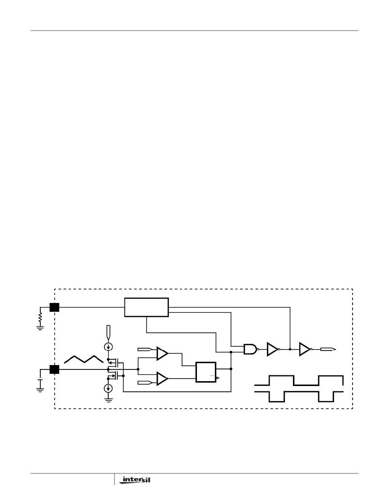
�?� Clock� Generator� (CT,� RD)�
�-� This� free-running� oscillator� is� set� by� two� external�
�components� as� shown� in� Figure� 1.� A� capacitor� at� CT� is�
�charged� and� discharged� with� two� equal� constant� current�
�sources� and� fed� into� a� window� comparator� to� set� the� clock�
�frequency.� A� resistor� at� RD� sets� the� clock� dead� time.� RD�
�and� CT� should� be� tied� to� the� VSS� pin� on� their� other� ends�
�as� close� as� possible.� The� corresponding� CT� for� a� particular�
�frequency� can� be� selected� from� Figure� 2.�
�-� The� switching� frequency� (Fsw)� of� the� power� train� is� half� of�
�the� clock� frequency� (Fclock),� as� shown� in� Equation� 1.�
�Fsw� =� -------------------�
�RETURNs� of� external� drivers� as� close� as� possible� with�
�heavy� copper� traces.�
�-� Copper� planes� should� be� attached� to� both� pins.�
�RD�
�SET� CLOCK�
�DEAD� TIME� (DT)�
�RD�
�VDD-�
�Fclock�
�2�
�(EQ.� 1)�
�I_CT�
�VMAX�
�-�
�OUT�
�CLK�
�+�
�CT�
�CT�
�VMIN�
�-� OUT�
�+�
�S�
�R�
�Q�
�Q�
�Q�
�Q�
�I_CT�
�10�
�CLK�
�FIGURE� 1.� SIMPLIFIED� CLOCK� GENERATOR� CIRCUIT�
�DT�
�DT�
�FN9066.5�
�January� 3,� 2006�
�相关PDF资料 |
PDF描述 |
|---|---|
| ISL6552CR-T | IC REG CTRLR BUCK PWM 20-QFN |
| ISL6553CB-T | IC REG CTRLR BUCK PWM 16-SOIC |
| ISL6554CB-T | IC PWM CORE VOLTAGE REG 20-SOIC |
| ISL6556ACR-T | IC CTRLR MULTIPHASE VRM10 32-QFN |
| ISL6556BCR-T | IC CTRLR MULTIPHASE VRM10 32-QFN |
相关代理商/技术参数 |
参数描述 |
|---|---|
| ISL6551IRZ | 功能描述:IC REG CTRLR FLYBACK PWM 28-QFN RoHS:是 类别:集成电路 (IC) >> PMIC - 稳压器 - DC DC 切换控制器 系列:- 标准包装:4,000 系列:- PWM 型:电压模式 输出数:1 频率 - 最大:1.5MHz 占空比:66.7% 电源电压:4.75 V ~ 5.25 V 降压:是 升压:无 回扫:无 反相:无 倍增器:无 除法器:无 Cuk:无 隔离:无 工作温度:-40°C ~ 85°C 封装/外壳:40-VFQFN 裸露焊盘 包装:带卷 (TR) |
| ISL6552CB | 功能描述:IC REG CTRLR BUCK PWM 20-SOIC RoHS:否 类别:集成电路 (IC) >> PMIC - 稳压器 - DC DC 切换控制器 系列:- 标准包装:4,000 系列:- PWM 型:电压模式 输出数:1 频率 - 最大:1.5MHz 占空比:66.7% 电源电压:4.75 V ~ 5.25 V 降压:是 升压:无 回扫:无 反相:无 倍增器:无 除法器:无 Cuk:无 隔离:无 工作温度:-40°C ~ 85°C 封装/外壳:40-VFQFN 裸露焊盘 包装:带卷 (TR) |
| ISL6552CB-T | 功能描述:IC REG CTRLR BUCK PWM 20-SOIC RoHS:否 类别:集成电路 (IC) >> PMIC - 稳压器 - DC DC 切换控制器 系列:- 标准包装:4,000 系列:- PWM 型:电压模式 输出数:1 频率 - 最大:1.5MHz 占空比:66.7% 电源电压:4.75 V ~ 5.25 V 降压:是 升压:无 回扫:无 反相:无 倍增器:无 除法器:无 Cuk:无 隔离:无 工作温度:-40°C ~ 85°C 封装/外壳:40-VFQFN 裸露焊盘 包装:带卷 (TR) |
| ISL6552CBZ | 功能描述:IC REG CTRLR BUCK PWM 20-SOIC RoHS:是 类别:集成电路 (IC) >> PMIC - 稳压器 - DC DC 切换控制器 系列:- 产品培训模块:Lead (SnPb) Finish for COTS Obsolescence Mitigation Program 标准包装:2,500 系列:- PWM 型:电流模式 输出数:1 频率 - 最大:275kHz 占空比:50% 电源电压:18 V ~ 110 V 降压:无 升压:无 回扫:无 反相:无 倍增器:无 除法器:无 Cuk:无 隔离:是 工作温度:-40°C ~ 85°C 封装/外壳:8-SOIC(0.154",3.90mm 宽) 包装:带卷 (TR) |
| ISL6552CBZA | 功能描述:IC REG CTRLR BUCK PWM 20-SOIC RoHS:是 类别:集成电路 (IC) >> PMIC - 稳压器 - DC DC 切换控制器 系列:- 产品培训模块:Lead (SnPb) Finish for COTS Obsolescence Mitigation Program 标准包装:2,500 系列:- PWM 型:电流模式 输出数:1 频率 - 最大:275kHz 占空比:50% 电源电压:18 V ~ 110 V 降压:无 升压:无 回扫:无 反相:无 倍增器:无 除法器:无 Cuk:无 隔离:是 工作温度:-40°C ~ 85°C 封装/外壳:8-SOIC(0.154",3.90mm 宽) 包装:带卷 (TR) |
发布紧急采购,3分钟左右您将得到回复。