参数资料
| 型号: | ISL6556BCB-T |
| 厂商: | Intersil |
| 文件页数: | 12/24页 |
| 文件大小: | 0K |
| 描述: | IC CTRLR MULTIPHASE VRM10 28SOIC |
| 标准包装: | 1,000 |
| 应用: | 控制器,Intel VR10X |
| 输入电压: | 3 V ~ 12 V |
| 输出数: | 4 |
| 输出电压: | 0.84 V ~ 1.6 V |
| 工作温度: | 0°C ~ 70°C |
| 安装类型: | 表面贴装 |
| 封装/外壳: | 28-SOIC(0.295",7.50mm 宽) |
| 供应商设备封装: | 28-SOIC W |
| 包装: | 带卷 (TR) |
�� �
�
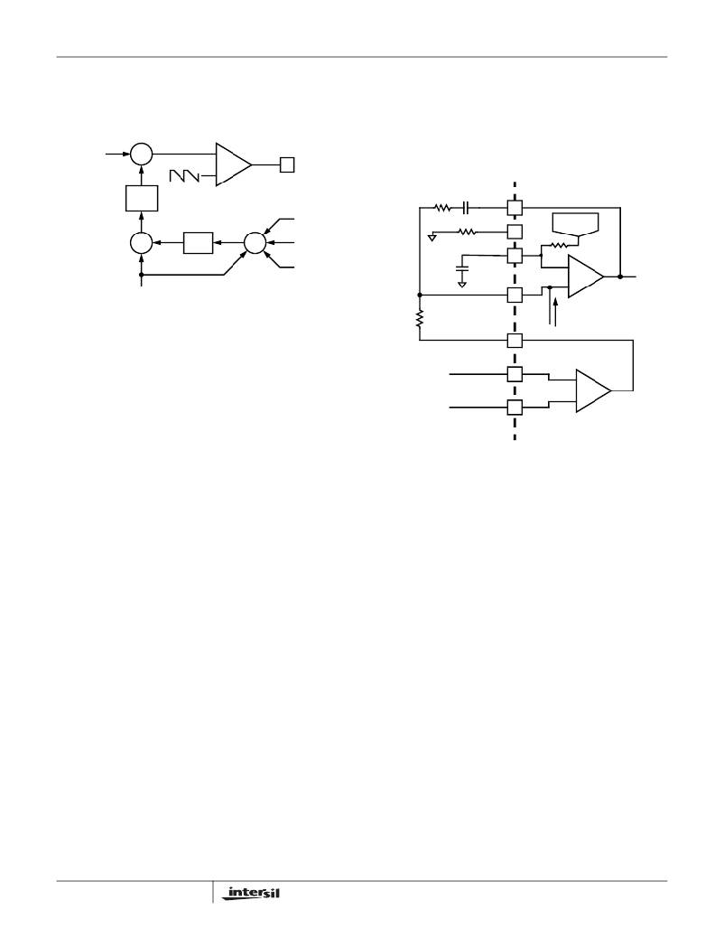
�ISL6556B�
�pulse� width� which� corrects� for� any� unbalance� and� drives� the�
�error� current� toward� zero.� Figure� 4� illustrates� Intersil’s�
�patented� current-balance� method� as� implemented� on�
�channel-1� of� a� multi-phase� converter.�
�The� output� of� the� error� amplifier,� V� COMP� ,� is� compared� to� the�
�sawtooth� waveform� to� generate� the� PWM� signals.� The� PWM�
�signals� control� the� timing� of� the� Intersil� MOSFET� drivers� and�
�regulate� the� converter� output� to� the� specified� reference�
�voltage.� The� internal� and� external� circuitry� that� controls�
�V� COMP�
�+�
�-�
�+�
�-�
�PWM1�
�voltage� regulation� is� illustrated� in� Figure� 5.�
�EXTERNAL� CIRCUIT�
�ISL6556B� INTERNAL� CIRCUIT�
�f(j� ω� )�
�SAWTOOTH� SIGNAL�
�R� C�
�C� C�
�COMP�
�I� ER�
�-�
�I� AVG�
�÷� N�
�Σ�
�I� 4� *�
�I� 3� *�
�T� COMP�
�R� TCOMP�
�REF�
�VID� DAC�
�1k�
�+�
�I� 2�
�C� REF�
�+�
�I� 1�
�FB�
�-�
�V� COMP�
�NOTE:� *Channels� 3� and� 4� are� optional.�
�FIGURE� 4.� CHANNEL-1� PWM� FUNCTION� AND� CURRENT-�
�R� FB�
�+�
�V� DROOP�
�-�
�VDIFF�
�ERROR� AMPLIFIER�
�I� AVG�
�BALANCE� ADJUSTMENT�
�Two� considerations� designers� face� are� MOSFET� selection�
�V� OUT� +�
�VSEN�
�+�
�and� inductor� design.� Both� are� significantly� improved� when�
�channel� currents� track� at� any� load� level.� The� need� for�
�complex� drive� schemes� for� multiple� MOSFETs,� exotic�
�magnetic� materials,� and� expensive� heat� sinks� is� avoided,�
�V� OUT� -�
�RGND�
�-�
�DIFFERENTIAL�
�REMOTE-SENSE�
�AMPLIFIER�
�resulting� in� a� cost-effective� and� easy-to-implement� solution�
�relative� to� single-phase� conversion.� Channel-current� balance�
�insures� that� the� thermal� advantage� of� multi-phase�
�conversion� is� realized.� Heat� dissipation� in� multiple� channels�
�is� spread� over� a� greater� area� than� can� easily� be�
�accomplished� using� the� single� phase� approach.�
�In� some� circumstances,� it� may� be� necessary� to� deliberately�
�design� some� channel-current� unbalance� into� the� system.� In�
�a� highly� compact� design,� one� or� two� channels� may� be� able� to�
�cool� more� effectively� than� the� other(s)� due� to� nearby� air� flow�
�or� heat� sinking� components.� The� other� channel(s)� may� have�
�more� difficulty� cooling� with� comparatively� less� air� flow� and�
�heat� sinking.� The� hotter� channels� may� also� be� located� close�
�to� other� heat-generating� components� tending� to� drive� their�
�temperature� even� higher.� In� these� cases,� the� proper�
�selection� of� the� current� sense� resistors� (R� ISEN� in� Figure� 3)�
�introduces� channel� current� unbalance� into� the� system.�
�Increasing� the� value� of� R� ISEN� in� the� cooler� channels� and�
�decreasing� it� in� the� hotter� channels� moves� all� channels� into�
�thermal� balance� at� the� expense� of� current� balance.�
�Voltage� Regulation�
�The� integrating� compensation� network� shown� in� Figure� 5�
�assures� that� the� steady-state� error� in� the� output� voltage� is�
�limited� only� to� the� error� in� the� reference� voltage� (output� of�
�the� DAC)� and� offset� errors� in� the� OFS� current� source,�
�remote-sense� and� error� amplifiers.� Intersil� specifies� the�
�guaranteed� tolerance� of� the� ISL6556B� to� include� the�
�combined� tolerances� of� each� of� these� elements.�
�12�
�FIGURE� 5.� OUTPUT� VOLTAGE� AND� LOAD-LINE�
�REGULATION� WITH� OFFSET� ADJUSTMENT�
�The� ISL6556B� incorporates� an� internal� differential� remote-�
�sense� amplifier� in� the� feedback� path.� The� amplifier� removes�
�the� voltage� error� encountered� when� measuring� the� output�
�voltage� relative� to� the� local� controller� ground� reference� point�
�resulting� in� a� more� accurate� means� of� sensing� output�
�voltage.� Connect� the� microprocessor� sense� pins� to� the� non-�
�inverting� input,� VSEN,� and� inverting� input,� RGND,� of� the�
�remote-sense� amplifier.� The� remote-sense� output,� V� DIFF� ,� is�
�connected� to� the� inverting� input� of� the� error� amplifier� through�
�an� external� resistor.�
�A� digital� to� analog� converter� (DAC)� generates� a� reference�
�voltage� based� on� the� state� of� logic� signals� at� pins� VID4�
�through� VID12.5.� The� DAC� decodes� the� 6-bit� logic� signal�
�(VID)� into� one� of� the� discrete� voltages� shown� in� Table� 1.�
�Each� VID� input� offers� a� 20� μ� A� pull-up� to� an� internal� 2.5V�
�source� for� use� with� open-drain� outputs.� The� pull-up� current�
�diminishes� to� zero� above� the� logic� threshold� to� protect�
�voltage-sensitive� output� devices.� External� pull-up� resistors�
�can� augment� the� pull-up� current� sources� in� case� leakage�
�into� the� driving� device� is� greater� than� 20� μ� A.�
�FN9097.4�
�December� 28,� 2004�
�相关PDF资料 |
PDF描述 |
|---|---|
| X5165V14I-2.7 | IC SUPERVISOR CPU 16K EE 14TSSOP |
| ESM28DTBS-S189 | CONN EDGECARD 56POS R/A .156 SLD |
| AMM12DTKH-S288 | CONN EDGECARD 24POS .156 EXTEND |
| X5165V14I | IC SUPERVISOR CPU 16K EE 14TSSOP |
| ISL6556BCB | IC CTRLR MULTIPHASE VRM10 28SOIC |
相关代理商/技术参数 |
参数描述 |
|---|---|
| ISL6556BCBZ | 功能描述:电流型 PWM 控制器 VRM 10 0 MULTI-PHS CONTROLLER RoHS:否 制造商:Texas Instruments 开关频率:27 KHz 上升时间: 下降时间: 工作电源电压:6 V to 15 V 工作电源电流:1.5 mA 输出端数量:1 最大工作温度:+ 105 C 安装风格:SMD/SMT 封装 / 箱体:TSSOP-14 |
| ISL6556BCBZ | 制造商:Intersil Corporation 功能描述:Pulse Width Modulation (PWM) Controller |
| ISL6556BCBZ-T | 功能描述:电流型 PWM 控制器 VRM 10 0 MULTI-PHS CONTROLLER RoHS:否 制造商:Texas Instruments 开关频率:27 KHz 上升时间: 下降时间: 工作电源电压:6 V to 15 V 工作电源电流:1.5 mA 输出端数量:1 最大工作温度:+ 105 C 安装风格:SMD/SMT 封装 / 箱体:TSSOP-14 |
| ISL6556BCR | 功能描述:IC CTRLR MULTIPHASE VRM10 32-QFN RoHS:否 类别:集成电路 (IC) >> PMIC - 稳压器 - 专用型 系列:- 产品培训模块:Lead (SnPb) Finish for COTS Obsolescence Mitigation Program 标准包装:2,000 系列:- 应用:电源,ICERA E400,E450 输入电压:4.1 V ~ 5.5 V 输出数:10 输出电压:可编程 工作温度:-40°C ~ 85°C 安装类型:表面贴装 封装/外壳:42-WFBGA,WLCSP 供应商设备封装:42-WLP 包装:带卷 (TR) |
| ISL6556BCRR5148 | 制造商:Rochester Electronics LLC 功能描述:- Bulk |
发布紧急采购,3分钟左右您将得到回复。