参数资料
| 型号: | ISL6559CBZ-T |
| 厂商: | Intersil |
| 文件页数: | 7/21页 |
| 文件大小: | 0K |
| 描述: | IC REG CTRLR BUCK PWM VM 28-SOIC |
| 标准包装: | 1 |
| PWM 型: | 电压模式 |
| 输出数: | 1 |
| 频率 - 最大: | 4MHz |
| 占空比: | 75% |
| 电源电压: | 4.75 V ~ 5.25 V |
| 降压: | 是 |
| 升压: | 无 |
| 回扫: | 无 |
| 反相: | 无 |
| 倍增器: | 无 |
| 除法器: | 无 |
| Cuk: | 无 |
| 隔离: | 无 |
| 工作温度: | 0°C ~ 70°C |
| 封装/外壳: | 28-SOIC(0.295",7.50mm 宽) |
| 包装: | 标准包装 |
| 产品目录页面: | 1243 (CN2011-ZH PDF) |
| 其它名称: | ISL6559CBZ-TDKR |
�� �
�
�ISL6559�
�To� understand� the� reduction� of� ripple� current� amplitude� in�
�the� multi-phase� circuit,� examine� the� equation� representing�
�an� individual� channel’s� peak-to-peak� inductor� current.�
�converter� has� 11.9A� RMS� input� capacitor� current.� The�
�single-phase� converter� must� use� an� input� capacitor� bank�
�with� twice� the� RMS� current� capacity� as� the� equivalent� three-�
�(� V� IN� –� V� OUT� )� V� OUT�
�I� PP� =� ------------------------------------------------------�
�L� f� S� V� IN�
�(EQ.� 1)�
�phase� converter.�
�Figures� 15,� 16� and� 17� in� the� section� entitled� Input� Capacitor�
�Selection� can� be� used� to� determine� the� input-capacitor� RMS�
�I� C� ,� PP� =� ------------------------------------------------------------�
�In� Equation� 1,� V� IN� and� V� OUT� are� the� input� and� output�
�voltages� respectively,� L� is� the� single-channel� inductor� value,�
�and� f� S� is� the� switching� frequency.�
�The� output� capacitors� conduct� the� ripple� component� of� the�
�inductor� current.� In� the� case� of� multi-phase� converters,� the�
�capacitor� current� is� the� sum� of� the� ripple� currents� from� each�
�of� the� individual� channels.� Compare� Equation� 1� to� the�
�expression� for� the� peak-to-peak� current� after� the� summation�
�of� N� symmetrically� phase-shifted� inductor� currents� in�
�Equation� 2.� Peak-to-peak� ripple� current� decreases� by� an�
�amount� proportional� to� the� number� of� channels.� Output-�
�voltage� ripple� is� a� function� of� capacitance,� capacitor�
�equivalent� series� resistance� (ESR),� and� inductor� ripple�
�current.� Reducing� the� inductor� ripple� current� allows� the�
�designer� to� use� fewer� or� less� costly� output� capacitors.�
�(� V� IN� –� N� V� OUT� )� V� OUT� (EQ.� 2)�
�L� f� S� V� IN�
�Another� benefit� of� interleaving� is� to� reduce� input� ripple�
�current.� Input� capacitance� is� determined� in� part� by� the�
�maximum� input� ripple� current.� Multi-phase� topologies� can�
�improve� overall� system� cost� and� size� by� lowering� input� ripple�
�current� and� allowing� the� designer� to� reduce� the� cost� of� input�
�capacitance.� The� example� in� Figure� 2� illustrates� input�
�currents� from� a� three-phase� converter� combining� to� reduce�
�the� total� input� ripple� current.�
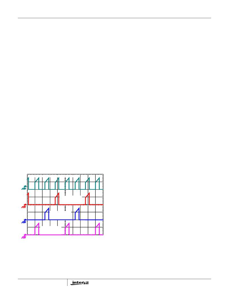
�INPUT-CAPACITOR CURRENT, 10A/DIV�
�CHANNEL� 3�
�INPUT� CURRENT�
�10A/DIV�
�CHANNEL� 2�
�INPUT� CURRENT�
�10A/DIV�
�CHANNEL� 1�
�INPUT� CURRENT�
�10A/DIV�
�1� μ� s/DIV�
�FIGURE� 2.� CHANNEL� INPUT� CURRENTS� AND� INPUT-�
�CAPACITOR� RMS� CURRENT� FOR� 3-PHASE�
�CONVERTER�
�The� converter� depicted� in� Figure� 2� delivers� 36A� to� a� 1.5V�
�load� from� a� 12V� input.� The� RMS� input� capacitor� current� is�
�5.9A.� Compare� this� to� a� single-phase� converter� also�
�stepping� down� 12V� to� 1.5V� at� 36A.� The� single-phase�
�7�
�current� based� on� load� current,� duty� cycle,� and� the� number� of�
�channels.� They� are� provided� as� aids� in� determining� the�
�optimal� input� capacitor� solution.� Figure� 18� shows� the� single�
�phase� input-capacitor� RMS� current� for� comparison.�
�PWM� Operation�
�The� timing� of� each� converter� leg� is� set� by� the� number� of�
�active� channels.� The� default� channel� setting� for� the� ISL6559�
�is� four.� One� switching� cycle� is� defined� as� the� time� between�
�PWM1� pulse� termination� signals.� The� pulse� termination�
�signal� is� an� internally� generated� clock� signal� which� triggers�
�the� falling� edge� of� PWM1.� The� cycle� time� of� the� pulse�
�termination� signal� is� the� inverse� of� the� switching� frequency�
�set� by� the� resistor� between� the� FS/DIS� pin� and� ground.� Each�
�cycle� begins� when� the� clock� signal� commands� the� channel-1�
�PWM� output� to� go� low.� The� PWM1� transition� signals� the�
�channel-1� MOSFET� driver� to� turn� off� the� channel-1� upper�
�MOSFET� and� turn� on� the� channel-1� synchronous� MOSFET.�
�In� the� default� channel� configuration,� the� PWM2� pulse�
�terminates� 1/4� of� a� cycle� after� PWM1.� The� PWM� 3� output�
�follows� another� 1/4� of� a� cycle� after� PWM2.� PWM4� terminates�
�another� 1/4� of� a� cycle� after� PWM3.�
�If� PWM3� is� connected� to� VCC,� then� two� channel� operation� is�
�selected� and� the� PWM2� pulse� terminates� 1/2� of� a� cycle� later.�
�Connecting� PWM4� to� VCC� selects� three� channel� operation�
�and� the� pulse-termination� times� are� spaced� in� 1/3� cycle�
�increments.�
�Once� a� PWM� signal� transitions� low,� it� is� held� low� for� a�
�minimum� of� 1/4� cycle.� This� forced� off� time� is� required� to�
�ensure� an� accurate� current� sample.� Current� sensing� is�
�described� in� the� next� section.� After� the� forced� off� time�
�expires,� the� PWM� output� is� enabled.� The� PWM� output� state�
�is� driven� by� the� position� of� the� error� amplifier� output� signal,�
�V� COMP� ,� minus� the� current� correction� signal� relative� to� the�
�sawtooth� ramp� as� illustrated� in� Figure� 1.� When� the� modified�
�V� COMP� voltage� crosses� the� sawtooth� ramp,� the� PWM� output�
�transitions� high.� The� MOSFET� driver� detects� the� change� in�
�state� of� the� PWM� signal� and� turns� off� the� synchronous�
�MOSFET� and� turns� on� the� upper� MOSFET.� The� PWM� signal�
�will� remain� high� until� the� pulse� termination� signal� marks� the�
�beginning� of� the� next� cycle� by� triggering� the� PWM� signal� low.�
�Current� Sensing�
�During� the� forced� off� time� following� a� PWM� transition� low,� the�
�controller� senses� channel� load� current� by� sampling� the�
�voltage� across� the� lower� MOSFET� r� DS(ON)� ,� see� Figure� 3.� A�
�ground-referenced� amplifier,� internal� to� the� ISL6559,�
�connects� to� the� PHASE� node� through� a� resistor,� R� ISEN� .� The�
�voltage� across� R� ISEN� is� equivalent� to� the� voltage� drop�
�FN9084.8�
�December� 29,� 2004�
�相关PDF资料 |
PDF描述 |
|---|---|
| ISL6561CR-T | IC CTRLR PWM MULTIPHASE 40-QFN |
| ISL6563IR-T | IC CTRLR PWM MULTIPHASE 24-QFN |
| ISL6564AIRZ | IC REG CTRLR BUCK PWM VM 40-QFN |
| ISL6564IR-T | IC REG CTRLR BUCK PWM VM 40-QFN |
| ISL6565BCV-T | IC REG CTRLR BUCK PWM VM 28TSSOP |
相关代理商/技术参数 |
参数描述 |
|---|---|
| ISL6559CR | 功能描述:IC REG CTRLR BUCK PWM VM 32-QFN RoHS:否 类别:集成电路 (IC) >> PMIC - 稳压器 - DC DC 切换控制器 系列:- 标准包装:4,000 系列:- PWM 型:电压模式 输出数:1 频率 - 最大:1.5MHz 占空比:66.7% 电源电压:4.75 V ~ 5.25 V 降压:是 升压:无 回扫:无 反相:无 倍增器:无 除法器:无 Cuk:无 隔离:无 工作温度:-40°C ~ 85°C 封装/外壳:40-VFQFN 裸露焊盘 包装:带卷 (TR) |
| ISL6559CR-T | 功能描述:IC REG CTRLR BUCK PWM VM 32-QFN RoHS:否 类别:集成电路 (IC) >> PMIC - 稳压器 - DC DC 切换控制器 系列:- 标准包装:4,000 系列:- PWM 型:电压模式 输出数:1 频率 - 最大:1.5MHz 占空比:66.7% 电源电压:4.75 V ~ 5.25 V 降压:是 升压:无 回扫:无 反相:无 倍增器:无 除法器:无 Cuk:无 隔离:无 工作温度:-40°C ~ 85°C 封装/外壳:40-VFQFN 裸露焊盘 包装:带卷 (TR) |
| ISL6559CRZ | 功能描述:电流型 PWM 控制器 2 TO 4 PHS BUCK CNTRLR 32L 5X5 MLFP RoHS:否 制造商:Texas Instruments 开关频率:27 KHz 上升时间: 下降时间: 工作电源电压:6 V to 15 V 工作电源电流:1.5 mA 输出端数量:1 最大工作温度:+ 105 C 安装风格:SMD/SMT 封装 / 箱体:TSSOP-14 |
| ISL6559CRZR5265 | 功能描述:IC REG CTRLR BUCK PWM VM 32-QFN RoHS:是 类别:集成电路 (IC) >> PMIC - 稳压器 - DC DC 切换控制器 系列:- 产品培训模块:Lead (SnPb) Finish for COTS Obsolescence Mitigation Program 标准包装:2,500 系列:- PWM 型:电流模式 输出数:1 频率 - 最大:275kHz 占空比:50% 电源电压:18 V ~ 110 V 降压:无 升压:无 回扫:无 反相:无 倍增器:无 除法器:无 Cuk:无 隔离:是 工作温度:-40°C ~ 85°C 封装/外壳:8-SOIC(0.154",3.90mm 宽) 包装:带卷 (TR) |
| ISL6559CRZ-T | 功能描述:电流型 PWM 控制器 2 TO 4 PHS BUCK CNTRLR 32L 5X5 MLFP RoHS:否 制造商:Texas Instruments 开关频率:27 KHz 上升时间: 下降时间: 工作电源电压:6 V to 15 V 工作电源电流:1.5 mA 输出端数量:1 最大工作温度:+ 105 C 安装风格:SMD/SMT 封装 / 箱体:TSSOP-14 |
发布紧急采购,3分钟左右您将得到回复。