参数资料
| 型号: | ISL6566CRZ-T |
| 厂商: | Intersil |
| 文件页数: | 11/29页 |
| 文件大小: | 0K |
| 描述: | IC CTLR PWM BUCK 3PHASE 40-QFN |
| 标准包装: | 1 |
| 应用: | 控制器,Intel VRM9,VRM10,AMD Hammer 应用 |
| 输入电压: | 3 V ~ 12 V |
| 输出数: | 1 |
| 输出电压: | 0.8 V ~ 1.6 V |
| 工作温度: | 0°C ~ 70°C |
| 安装类型: | 表面贴装 |
| 封装/外壳: | 40-VFQFN 裸露焊盘 |
| 供应商设备封装: | 40-QFN(6x6) |
| 包装: | 标准包装 |
| 其它名称: | ISL6566CRZ-TDKR |
第1页第2页第3页第4页第5页第6页第7页第8页第9页第10页当前第11页第12页第13页第14页第15页第16页第17页第18页第19页第20页第21页第22页第23页第24页第25页第26页第27页第28页第29页
�� �
�
�ISL6566�
�Figures� 22� and� 23� in� the� section� entitled� Input� Capacitor�
�Selection� can� be� used� to� determine� the� input-capacitor� RMS�
�current� based� on� load� current,� duty� cycle,� and� the� number� of�
�channels.� They� are� provided� as� aids� in� determining� the�
�optimal� input� capacitor� solution.�
�PWM� Operation�
�The� timing� of� each� converter� leg� is� set� by� the� number� of�
�active� channels.� The� default� channel� setting� for� the� ISL6566�
�is� three.� One� switching� cycle� is� defined� as� the� time� between�
�the� internal� PWM1� pulse� termination� signals.� The� pulse�
�termination� signal� is� the� internally� generated� clock� signal�
�that� triggers� the� falling� edge� of� PWM1.� The� cycle� time� of� the�
�pulse� termination� signal� is� the� inverse� of� the� switching�
�frequency� set� by� the� resistor� between� the� FS� pin� and�
�ground.� Each� cycle� begins� when� the� clock� signal� commands�
�PWM1� to� go� low.� The� PWM1� transition� signals� the� internal�
�channel-1� MOSFET� driver� to� turn� off� the� channel-1� upper�
�from� each� active� channel� are� summed� together� and� divided�
�by� the� number� of� active� channels.� The� resulting� cycle�
�average� current,� I� AVG� ,� provides� a� measure� of� the� total� load-�
�current� demand� on� the� converter� during� each� switching�
�cycle.� Channel-current� balance� is� achieved� by� comparing�
�the� sampled� current� of� each� channel� to� the� cycle� average�
�current,� and� making� the� proper� adjustment� to� each� channel�
�pulse� width� based� on� the� error.� Intersil’s� patented� current-�
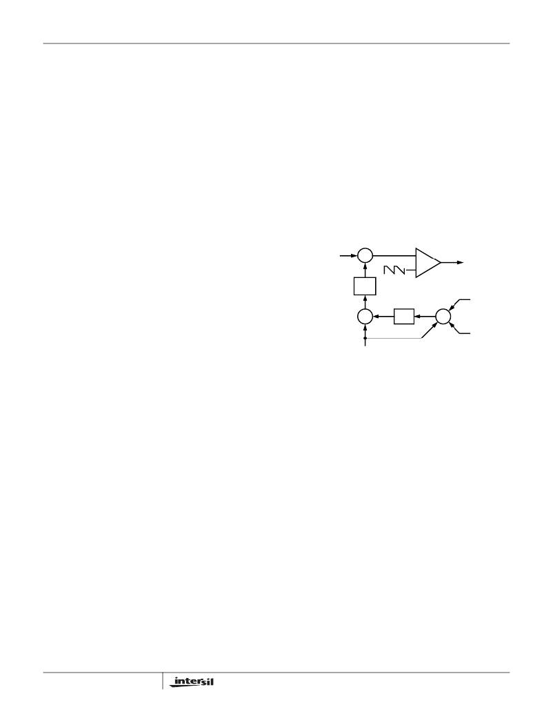
�balance� method� is� illustrated� in� Figure� 3,� with� error�
�correction� for� channel� 1� represented.� In� the� figure,� the� cycle�
�average� current,� I� AVG� ,� is� compared� with� the� channel� 1�
�sample,� I� 1� ,� to� create� an� error� signal� I� ER� .�
�The� filtered� error� signal� modifies� the� pulse� width�
�commanded� by� V� COMP� to� correct� any� unbalance� and� force�
�I� ER� toward� zero.� The� same� method� for� error� signal�
�correction� is� applied� to� each� active� channel.�
�MOSFET� and� turn� on� the� channel-1� synchronous� MOSFET.�
�In� the� default� channel� configuration,� the� PWM2� pulse�
�terminates� 1/3� of� a� cycle� after� the� PWM1� pulse.� The� PWM3�
�V� COMP�
�+�
�-�
�+�
�-�
�PWM1�
�TO� GATE�
�CONTROL�
�LOGIC�
�pulse� terminates� 1/3� of� a� cycle� after� PWM2.�
�FILTER�
�f(s)�
�SAWTOOTH� SIGNAL�
�If� PVCC3� is� left� open� or� connected� to� ground,� two� channel�
�operation� is� selected� and� the� PWM2� pulse� terminates� 1/2� of�
�a� cycle� after� the� PWM1� pulse� terminates.� If� both� PVCC3� and�
�PVCC2� are� left� open� or� connected� to� ground,� single� channel�
�operation� is� selected.�
�I� ER�
�+�
�-�
�I� AVG�
�÷� N�
�Σ�
�I� 3�
�I� 2�
�Once� a� PWM� pulse� transitions� low,� it� is� held� low� for� a�
�minimum� of� 1/3� cycle.� This� forced� off� time� is� required� to�
�ensure� an� accurate� current� sample.� Current� sensing� is�
�described� in� the� next� section.� After� the� forced� off� time�
�expires,� the� PWM� output� is� enabled.� The� PWM� output� state�
�is� driven� by� the� position� of� the� error� amplifier� output� signal,�
�V� COMP� ,� minus� the� current� correction� signal� relative� to� the�
�sawtooth� ramp� as� illustrated� in� Figure� 3.� When� the� modified�
�V� COMP� voltage� crosses� the� sawtooth� ramp,� the� PWM� output�
�transitions� high.� The� internal� MOSFET� driver� detects� the�
�change� in� state� of� the� PWM� signal� and� turns� off� the�
�synchronous� MOSFET� and� turns� on� the� upper� MOSFET.�
�The� PWM� signal� will� remain� high� until� the� pulse� termination�
�signal� marks� the� beginning� of� the� next� cycle� by� triggering� the�
�PWM� signal� low.�
�Channel-Current� Balance�
�One� important� benefit� of� multi-phase� operation� is� the� thermal�
�advantage� gained� by� distributing� the� dissipated� heat� over�
�multiple� devices� and� greater� area.� By� doing� this� the� designer�
�avoids� the� complexity� of� driving� parallel� MOSFETs� and� the�
�expense� of� using� expensive� heat� sinks� and� exotic� magnetic�
�materials.�
�In� order� to� realize� the� thermal� advantage,� it� is� important� that�
�each� channel� in� a� multi-phase� converter� be� controlled� to�
�carry� about� the� same� amount� of� current� at� any� load� level.� To�
�achieve� this,� the� currents� through� each� channel� must� be�
�sampled� every� switching� cycle.� The� sampled� currents,� I� n� ,�
�11�
�I� 1�
�NOTE:� Channel� 2� and� 3� are� optional.�
�FIGURE� 3.� CHANNEL-1� PWM� FUNCTION� AND� CURRENT-�
�BALANCE� ADJUSTMENT�
�Current� Sampling�
�In� order� to� realize� proper� current-balance,� the� currents� in�
�each� channel� must� be� sampled� every� switching� cycle.� This�
�sampling� occurs� during� the� forced� off-time,� following� a� PWM�
�transition� low.� During� this� time� the� current-sense� amplifier�
�uses� the� ISEN� inputs� to� reproduce� a� signal� proportional� to�
�the� inductor� current,� I� L� .� This� sensed� current,� I� SEN� ,� is� simply�
�a� scaled� version� of� the� inductor� current.� The� sample� window�
�opens� exactly� 1/6� of� the� switching� period,� t� SW� ,� after� the�
�PWM� transitions� low.� The� sample� window� then� stays� open�
�the� rest� of� the� switching� cycle� until� PWM� transitions� high�
�again,� as� illustrated� in� Figure� 4.�
�The� sampled� current,� at� the� end� of� the� t� SAMPLE� ,� is�
�proportional� to� the� inductor� current� and� is� held� until� the� next�
�switching� period� sample.� The� sampled� current� is� used� only�
�for� channel-current� balance.�
�FN9178.4�
�March� 9,� 2006�
�相关PDF资料 |
PDF描述 |
|---|---|
| ISL6567CRZ | IC REG CTRLR BUCK PWM VM 24-QFN |
| ISL6568CRZ-T | IC CTLR PWM BUCK 2PHASE 32-QFN |
| ISL6569ACR-T | IC REG CTRLR BUCK PWM 32-QFN |
| ISL6569CR-T | IC REG CTRLR DIVIDER PWM 32-QFN |
| ISL6571CRZ | IC MOSF DRVR/SYNC SW COMPL 68QFN |
相关代理商/技术参数 |
参数描述 |
|---|---|
| ISL6566CRZ-TR5184 | 功能描述:IC CTRLR PWM 3PHASE BUCK 40-QFN RoHS:是 类别:集成电路 (IC) >> PMIC - 稳压器 - 专用型 系列:- 标准包装:2,000 系列:- 应用:控制器,DSP 输入电压:4.5 V ~ 25 V 输出数:2 输出电压:最低可调至 1.2V 工作温度:-40°C ~ 85°C 安装类型:表面贴装 封装/外壳:30-TFSOP(0.173",4.40mm 宽) 供应商设备封装:30-TSSOP 包装:带卷 (TR) |
| ISL6566EVAL1 | 功能描述:EVAL BOARD 1 FOR ISL6566 RoHS:否 类别:编程器,开发系统 >> 评估板 - 线性稳压器 (LDO) 系列:* 产品变化通告:1Q2012 Discontinuation 30/Mar/2012 设计资源:NCP590MNDPTAGEVB Gerber Files 标准包装:1 系列:- 每 IC 通道数:2 - 双 输出电压:1.8V,2.8V 电流 - 输出:300mA 输入电压:2.1 ~ 5.5 V 稳压器类型:正,固定式 工作温度:-40°C ~ 85°C 板类型:完全填充 已供物品:板 已用 IC / 零件:NCP590MNDP 其它名称:NCP590MNDPTAGEVB-NDNCP590MNDPTAGEVBOS |
| ISL6566IR | 功能描述:IC CTRLR PWM BUCK 3PHASE 40-QFN RoHS:否 类别:集成电路 (IC) >> PMIC - 稳压器 - 专用型 系列:- 产品培训模块:Lead (SnPb) Finish for COTS Obsolescence Mitigation Program 标准包装:2,000 系列:- 应用:电源,ICERA E400,E450 输入电压:4.1 V ~ 5.5 V 输出数:10 输出电压:可编程 工作温度:-40°C ~ 85°C 安装类型:表面贴装 封装/外壳:42-WFBGA,WLCSP 供应商设备封装:42-WLP 包装:带卷 (TR) |
| ISL6566IR-T | 功能描述:IC CTRLR PWM BUCK 3PHASE 40-QFN RoHS:否 类别:集成电路 (IC) >> PMIC - 稳压器 - 专用型 系列:- 产品培训模块:Lead (SnPb) Finish for COTS Obsolescence Mitigation Program 标准包装:2,000 系列:- 应用:电源,ICERA E400,E450 输入电压:4.1 V ~ 5.5 V 输出数:10 输出电压:可编程 工作温度:-40°C ~ 85°C 安装类型:表面贴装 封装/外壳:42-WFBGA,WLCSP 供应商设备封装:42-WLP 包装:带卷 (TR) |
| ISL6566IRZ | 功能描述:IC CTRLR PWM BUCK 3PHASE 40-QFN RoHS:是 类别:集成电路 (IC) >> PMIC - 稳压器 - 专用型 系列:- 标准包装:43 系列:- 应用:控制器,Intel VR11 输入电压:5 V ~ 12 V 输出数:1 输出电压:0.5 V ~ 1.6 V 工作温度:-40°C ~ 85°C 安装类型:表面贴装 封装/外壳:48-VFQFN 裸露焊盘 供应商设备封装:48-QFN(7x7) 包装:管件 |
发布紧急采购,3分钟左右您将得到回复。