参数资料
| 型号: | ISL6566CRZ-T |
| 厂商: | Intersil |
| 文件页数: | 20/29页 |
| 文件大小: | 0K |
| 描述: | IC CTLR PWM BUCK 3PHASE 40-QFN |
| 标准包装: | 1 |
| 应用: | 控制器,Intel VRM9,VRM10,AMD Hammer 应用 |
| 输入电压: | 3 V ~ 12 V |
| 输出数: | 1 |
| 输出电压: | 0.8 V ~ 1.6 V |
| 工作温度: | 0°C ~ 70°C |
| 安装类型: | 表面贴装 |
| 封装/外壳: | 40-VFQFN 裸露焊盘 |
| 供应商设备封装: | 40-QFN(6x6) |
| 包装: | 标准包装 |
| 其它名称: | ISL6566CRZ-TDKR |
第1页第2页第3页第4页第5页第6页第7页第8页第9页第10页第11页第12页第13页第14页第15页第16页第17页第18页第19页当前第20页第21页第22页第23页第24页第25页第26页第27页第28页第29页
�� �
�
�ISL6566�
�If� VSEN� or� RGND� become� opened,� VDIFF� falls,� causing� the�
�duty� cycle� to� increase� and� the� output� voltage� on� IREF� to�
�increase.� If� the� voltage� on� IREF� exceeds� “VDIFF+1V”,� the�
�controller� will� shut� down.� Once� the� voltage� on� IREF� falls�
�below� “VDIFF+1V”,� the� ISL6566� will� restart� at� the� beginning�
�of� soft-start.�
�Overcurrent� Protection�
�The� ISL6566� detects� overcurrent� events� by� comparing� the�
�droop� voltage,� V� DROOP� ,� to� the� OCSET� voltage,� V� OCSET� ,� as�
�shown� in� Figure� 13.� The� droop� voltage,� set� by� the� external�
�current� sensing� circuitry,� is� proportional� to� the� output� current�
�as� shown� in� Equation� 7.� A� constant� 100� μ� A� flows� through�
�R� OCSET� ,� creating� the� OCSET� voltage.� When� the� droop�
�voltage� exceeds� the� OCSET� voltage,� the� overcurrent�
�protection� circuitry� activates.� Since� the� droop� voltage� is�
�proportional� to� the� output� current,� the� overcurrent� trip� level,�
�I� MAX� ,� can� be� set� by� selecting� the� proper� value� for� R� OCSET� ,�
�as� shown� in� Equation� 14.�
�power� converter.� It� is� assumed� that� the� reader� is� familiar� with�
�many� of� the� basic� skills� and� techniques� referenced� below.� In�
�addition� to� this� guide,� Intersil� provides� complete� reference�
�designs� that� include� schematics,� bills� of� materials,� and� example�
�board� layouts� for� all� common� microprocessor� applications.�
�Power� Stages�
�The� first� step� in� designing� a� multi-phase� converter� is� to�
�determine� the� number� of� phases.� This� determination�
�depends� heavily� on� the� cost� analysis� which� in� turn� depends�
�on� system� constraints� that� differ� from� one� design� to� the� next.�
�Principally,� the� designer� will� be� concerned� with� whether�
�components� can� be� mounted� on� both� sides� of� the� circuit�
�board,� whether� through-hole� components� are� permitted,� the�
�total� board� space� available� for� power-supply� circuitry,� and�
�the� maximum� amount� of� load� current.� Generally� speaking,�
�the� most� economical� solutions� are� those� in� which� each�
�phase� handles� between� 25� and� 30A.� All� surface-mount�
�designs� will� tend� toward� the� lower� end� of� this� current� range.�
�I� MAX� ?� R� COMP� ?� DCR�
�100� μ� ?� R� S�
�R� OCSET� =� ----------------------------------------------------------�
�(EQ.� 14)�
�If� through-hole� MOSFETs� and� inductors� can� be� used,� higher�
�per-phase� currents� are� possible.� In� cases� where� board�
�space� is� the� limiting� constraint,� current� can� be� pushed� as�
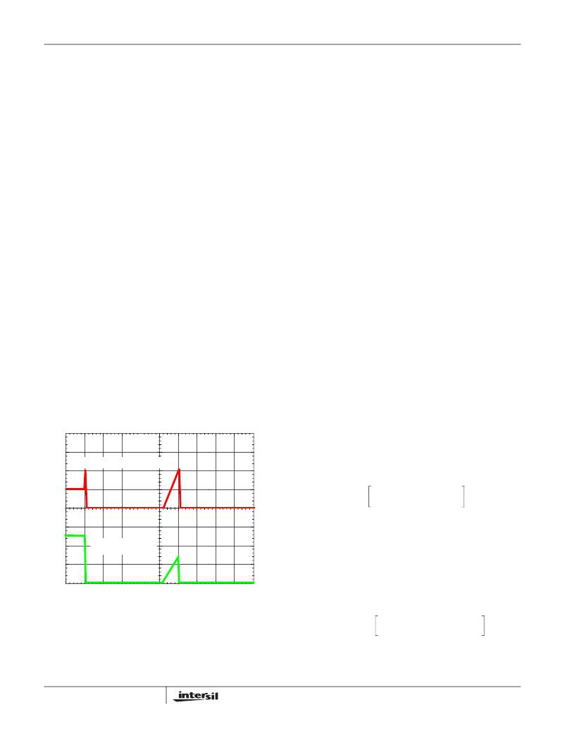
�Once� the� output� current� exceeds� the� overcurrent� trip� level,�
�V� DROOP� will� exceed� V� OCSET� ,� and� a� comparator� will� trigger� the�
�converter� to� begin� overcurrent� protection� procedures.� At� the�
�beginning� of� overcurrent� shutdown,� the� controller� turns� off� both�
�upper� and� lower� MOSFETs.� The� system� remains� in� this� state�
�for� a� period� of� 4096� switching� cycles.� If� the� controller� is� still�
�enabled� at� the� end� of� this� wait� period,� it� will� attempt� a� soft-start�
�(as� shown� in� Figure� 14).� If� the� fault� remains,� the� trip-retry� cycles�
�will� continue� indefinitely� until� either� the� controller� is� disabled� or�
�the� fault� is� cleared.� Note� that� the� energy� delivered� during� trip-�
�retry� cycling� is� much� less� than� during� full-load� operation,� so�
�there� is� no� thermal� hazard.�
�OUTPUT� CURRENT,� 50A/DIV�
�high� as� 40A� per� phase,� but� these� designs� require� heat� sinks�
�and� forced� air� to� cool� the� MOSFETs,� inductors� and� heat-�
�dissipating� surfaces.�
�MOSFETS�
�The� choice� of� MOSFETs� depends� on� the� current� each�
�MOSFET� will� be� required� to� conduct,� the� switching� frequency,�
�the� capability� of� the� MOSFETs� to� dissipate� heat,� and� the�
�availability� and� nature� of� heat� sinking� and� air� flow.�
�LOWER� MOSFET� POWER� CALCULATION�
�The� calculation� for� power� loss� in� the� lower� MOSFET� is�
�simple,� since� virtually� all� of� the� loss� in� the� lower� MOSFET� is�
�due� to� current� conducted� through� the� channel� resistance�
�(r� DS(ON)� ).� In� Equation� 15,� I� M� is� the� maximum� continuous�
�output� current,� I� PP� is� the� peak-to-peak� inductor� current� (see�
�Equation� 1),� and� d� is� the� duty� cycle� (V� OUT� /V� IN� ).�
�?� I� M� ?� 2� I� L� ,� PP� (� 1� –� d� )�
�P� LOW� ,� 1� =� r� DS� (� ON� )� ?� ------� ?� (� 1� –� d� )� +� --------------------------------�
�0A�
�?� N� ?� 12�
�(EQ.� 15)�
�An� additional� term� can� be� added� to� the� lower-MOSFET� loss�
�OUTPUT� VOLTAGE,�
�500mV/DIV�
�equation� to� account� for� additional� loss� accrued� during� the�
�dead� time� when� inductor� current� is� flowing� through� the�
�lower-MOSFET� body� diode.� This� term� is� dependent� on� the�
�0V�
�2ms/DIV�
�diode� forward� voltage� at� I� M� ,� V� D(ON)� ,� the� switching�
�frequency,� f� S� ,� and� the� length� of� dead� times,� t� d1� and� t� d2� ,� at�
�the� beginning� and� the� end� of� the� lower-MOSFET� conduction�
�P� LOW� ,� 2� =� V� D� (� ON� )� f� S� ?� ------� +� I� ---------� ?� t�
�I� PP� ?�
�?� I�
�d1� +� ?� ------� –� ---------� ?� t� d2�
�FIGURE� 14.� OVERCURRENT� BEHAVIOR� IN� HICCUP� MODE�
�F� SW� =� 500kHz�
�General� Design� Guide�
�interval� respectively.�
�I� M� PP�
�?� N� 2� ?�
�M�
�?� N� 2� ?�
�(EQ.� 16)�
�This� design� guide� is� intended� to� provide� a� high-level�
�explanation� of� the� steps� necessary� to� create� a� multi-phase�
�20�
�The� total� maximum� power� dissipated� in� each� lower� MOSFET�
�is� approximated� by� the� summation� of� P� LOW,1� and� P� LOW,2� .�
�FN9178.4�
�March� 9,� 2006�
�相关PDF资料 |
PDF描述 |
|---|---|
| ISL6567CRZ | IC REG CTRLR BUCK PWM VM 24-QFN |
| ISL6568CRZ-T | IC CTLR PWM BUCK 2PHASE 32-QFN |
| ISL6569ACR-T | IC REG CTRLR BUCK PWM 32-QFN |
| ISL6569CR-T | IC REG CTRLR DIVIDER PWM 32-QFN |
| ISL6571CRZ | IC MOSF DRVR/SYNC SW COMPL 68QFN |
相关代理商/技术参数 |
参数描述 |
|---|---|
| ISL6566CRZ-TR5184 | 功能描述:IC CTRLR PWM 3PHASE BUCK 40-QFN RoHS:是 类别:集成电路 (IC) >> PMIC - 稳压器 - 专用型 系列:- 标准包装:2,000 系列:- 应用:控制器,DSP 输入电压:4.5 V ~ 25 V 输出数:2 输出电压:最低可调至 1.2V 工作温度:-40°C ~ 85°C 安装类型:表面贴装 封装/外壳:30-TFSOP(0.173",4.40mm 宽) 供应商设备封装:30-TSSOP 包装:带卷 (TR) |
| ISL6566EVAL1 | 功能描述:EVAL BOARD 1 FOR ISL6566 RoHS:否 类别:编程器,开发系统 >> 评估板 - 线性稳压器 (LDO) 系列:* 产品变化通告:1Q2012 Discontinuation 30/Mar/2012 设计资源:NCP590MNDPTAGEVB Gerber Files 标准包装:1 系列:- 每 IC 通道数:2 - 双 输出电压:1.8V,2.8V 电流 - 输出:300mA 输入电压:2.1 ~ 5.5 V 稳压器类型:正,固定式 工作温度:-40°C ~ 85°C 板类型:完全填充 已供物品:板 已用 IC / 零件:NCP590MNDP 其它名称:NCP590MNDPTAGEVB-NDNCP590MNDPTAGEVBOS |
| ISL6566IR | 功能描述:IC CTRLR PWM BUCK 3PHASE 40-QFN RoHS:否 类别:集成电路 (IC) >> PMIC - 稳压器 - 专用型 系列:- 产品培训模块:Lead (SnPb) Finish for COTS Obsolescence Mitigation Program 标准包装:2,000 系列:- 应用:电源,ICERA E400,E450 输入电压:4.1 V ~ 5.5 V 输出数:10 输出电压:可编程 工作温度:-40°C ~ 85°C 安装类型:表面贴装 封装/外壳:42-WFBGA,WLCSP 供应商设备封装:42-WLP 包装:带卷 (TR) |
| ISL6566IR-T | 功能描述:IC CTRLR PWM BUCK 3PHASE 40-QFN RoHS:否 类别:集成电路 (IC) >> PMIC - 稳压器 - 专用型 系列:- 产品培训模块:Lead (SnPb) Finish for COTS Obsolescence Mitigation Program 标准包装:2,000 系列:- 应用:电源,ICERA E400,E450 输入电压:4.1 V ~ 5.5 V 输出数:10 输出电压:可编程 工作温度:-40°C ~ 85°C 安装类型:表面贴装 封装/外壳:42-WFBGA,WLCSP 供应商设备封装:42-WLP 包装:带卷 (TR) |
| ISL6566IRZ | 功能描述:IC CTRLR PWM BUCK 3PHASE 40-QFN RoHS:是 类别:集成电路 (IC) >> PMIC - 稳压器 - 专用型 系列:- 标准包装:43 系列:- 应用:控制器,Intel VR11 输入电压:5 V ~ 12 V 输出数:1 输出电压:0.5 V ~ 1.6 V 工作温度:-40°C ~ 85°C 安装类型:表面贴装 封装/外壳:48-VFQFN 裸露焊盘 供应商设备封装:48-QFN(7x7) 包装:管件 |
发布紧急采购,3分钟左右您将得到回复。