- 您现在的位置:买卖IC网 > PDF目录20648 > ISL6605CRZ-T (Intersil)IC MOSFET DRVR SYNC BUCK 8-QFN PDF资料下载
参数资料
| 型号: | ISL6605CRZ-T |
| 厂商: | Intersil |
| 文件页数: | 5/9页 |
| 文件大小: | 0K |
| 描述: | IC MOSFET DRVR SYNC BUCK 8-QFN |
| 标准包装: | 6,000 |
| 配置: | 高端和低端,同步 |
| 输入类型: | PWM |
| 电流 - 峰: | 2A |
| 配置数: | 1 |
| 输出数: | 2 |
| 高端电压 - 最大(自引导启动): | 33V |
| 电源电压: | 4.5 V ~ 5.5 V |
| 工作温度: | 0°C ~ 70°C |
| 安装类型: | 表面贴装 |
| 封装/外壳: | 8-VQFN 裸露焊盘 |
| 供应商设备封装: | 8-QFN(3x3) |
| 包装: | 带卷 (TR) |
�� �
�
�ISL6605�
�Functional� Pin� Description�
�Note:� Pin� numbers� refer� to� the� SOIC� package.� Check�
�PINOUT� diagrams� for� QFN� pin� numbers.�
�UGATE� (Pin� 1)�
�Upper� gate� drive� output.� Connect� to� gate� of� high-side� power�
�N-Channel� MOSFET.�
�BOOT� (Pin� 2)�
�Floating� bootstrap� supply� pin� for� the� upper� gate� drive.�
�Connect� the� bootstrap� capacitor� between� this� pin� and� the�
�PHASE� pin.� The� bootstrap� capacitor� provides� the� charge� to�
�turn� on� the� upper� MOSFET.� See� the� Bootstrap� Diode� and�
�Capacitor� section� under� DESCRIPTION� for� guidance� in�
�choosing� the� appropriate� capacitor� value.�
�PWM� (Pin� 3)�
�The� PWM� signal� is� the� control� input� for� the� driver.� The� PWM�
�signal� can� enter� three� distinct� states� during� operation� (see� the�
�three-state� PWM� Input� section� under� DESCRIPTION� for� further�
�details).� Connect� this� pin� to� the� PWM� output� of� the� controller.�
�GND� (Pin� 4)�
�Ground� pin.� All� signals� are� referenced� to� this� node.�
�LGATE� (Pin� 5)�
�Lower� gate� drive� output.� Connect� to� gate� of� the� low-side�
�power� N-Channel� MOSFET.�
�VCC� (Pin� 6)�
�Connect� this� pin� to� a� +5V� bias� supply.� Place� a� high� quality�
�bypass� capacitor� from� this� pin� to� GND.�
�EN� (Pin� 7)�
�Enable� input� pin.� Connect� this� pin� to� HIGH� to� enable� and�
�LOW� to� disable� the� IC.� When� disabled,� the� IC� draws� less�
�than� 1� μ� A� bias� current.�
�PHASE� (Pin� 8)�
�Connect� this� pin� to� the� source� of� the� upper� MOSFET� and� the�
�drain� of� the� lower� MOSFET.� This� pin� provides� a� return� path�
�for� the� upper� gate� driver.�
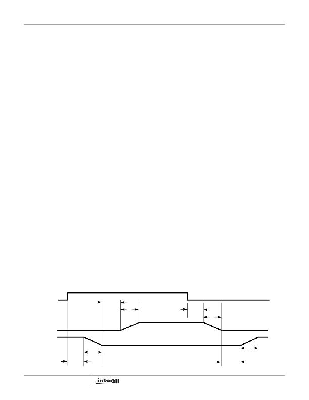
�Timing� Diagram�
�Thermal� Pad� (in� QFN� only)�
�In� the� QFN� package,� the� pad� underneath� the� center� of� the�
�IC� is� a� thermal� substrate.� The� PCB� “thermal� land”� design�
�for� this� exposed� die� pad� should� include� thermal� vias� that�
�drop� down� and� connect� to� one� or� more� buried� copper�
�plane(s).� This� combination� of� vias� for� vertical� heat� escape�
�and� buried� planes� for� heat� spreading� allows� the� QFN� to�
�achieve� its� full� thermal� potential.� This� pad� should� be� either�
�grounded� or� floating,� and� it� should� not� be� connected� to�
�other� nodes.� Refer� to� TB389� for� design� guidelines.�
�Description�
�Operation�
�Designed� for� speed,� the� ISL6605� MOSFET� driver� controls� both�
�high-side� and� low-side� N-Channel� FETs� from� one� externally�
�provided� PWM� signal.�
�A� rising� edge� on� PWM� initiates� the� turn-off� of� the� lower�
�MOSFET� (see� Timing� Diagram).� After� a� short� propagation�
�delay� [t� PDLLGATE� ],� the� lower� gate� begins� to� fall.� Typical� fall�
�times� [t� FLGATE� ]� are� provided� in� the� Electrical� Specifications�
�section.� Adaptive� shoot-through� circuitry� monitors� the�
�LGATE� voltage� and� determines� the� upper� gate� delay� time�
�[t� PDHUGATE� ]� based� on� how� quickly� the� LGATE� voltage�
�drops� below� 1V.� This� prevents� both� the� lower� and� upper�
�MOSFETs� from� conducting� simultaneously� or� shoot-�
�through.� Once� this� delay� period� is� completed� the� upper� gate�
�drive� begins� to� rise� [t� RUGATE� ]� and� the� upper� MOSFET� turns�
�on.�
�A� falling� transition� on� PWM� indicates� the� turn-off� of� the� upper�
�MOSFET� and� the� turn-on� of� the� lower� MOSFET.� A� short�
�propagation� delay� [t� PDLUGATE� ]� is� encountered� before� the�
�upper� gate� begins� to� fall� [t� FUGATE� ].� Again,� the� adaptive�
�shoot-through� circuitry� determines� the� lower� gate� delay� time,�
�t� PDHLGATE� .� The� upper� MOSFET� gate� voltage� is� monitored�
�and� the� lower� gate� is� allowed� to� rise� after� the� upper� MOSFET�
�gate-to-source� voltage� drops� below� 1V.� The� lower� gate� then�
�rises� [t� RLGATE� ],� turning� on� the� lower� MOSFET.�
�PWM�
�t� PDHUGATE�
�t� PDLUGATE�
�t� RUGATE�
�t� FUGATE�
�UGATE�
�LGATE�
�t� RLGATE�
�t� FLGATE�
�t� PDLLGATE�
�5�
�t� PDHLGATE�
�FN9091.7�
�May� 9,� 2006�
�相关PDF资料 |
PDF描述 |
|---|---|
| VE-BNW-EV-B1 | CONVERTER MOD DC/DC 5.5V 150W |
| MBRD640CTG | DIODE SCHOTTKY 40V 3A DPAK |
| VE-BNW-EU-F4 | CONVERTER MOD DC/DC 5.5V 200W |
| MBRB30H60CTT4G | DIODE SCHOTTKY 60V 15A H D2PAK |
| GEC10DRTS-S734 | CONN EDGECARD 20POS DIP .100 SLD |
相关代理商/技术参数 |
参数描述 |
|---|---|
| ISL6605CRZ-TK | 功能描述:IC MOSFET DVR SYNC BUCK 8QFN RoHS:是 类别:集成电路 (IC) >> PMIC - MOSFET,电桥驱动器 - 外部开关 系列:- 标准包装:6,000 系列:* |
| ISL6605IB | 功能描述:功率驱动器IC MOSFET DUAL SYNC RoHS:否 制造商:Micrel 产品:MOSFET Gate Drivers 类型:Low Cost High or Low Side MOSFET Driver 上升时间: 下降时间: 电源电压-最大:30 V 电源电压-最小:2.75 V 电源电流: 最大功率耗散: 最大工作温度:+ 85 C 安装风格:SMD/SMT 封装 / 箱体:SOIC-8 封装:Tube |
| ISL6605IB-T | 功能描述:IC MOSFET DRVR SYNC BUCK 8-SOIC RoHS:否 类别:集成电路 (IC) >> PMIC - MOSFET,电桥驱动器 - 外部开关 系列:- 标准包装:50 系列:- 配置:低端 输入类型:非反相 延迟时间:40ns 电流 - 峰:9A 配置数:1 输出数:1 高端电压 - 最大(自引导启动):- 电源电压:4.5 V ~ 35 V 工作温度:-40°C ~ 125°C 安装类型:表面贴装 封装/外壳:TO-263-6,D²Pak(5 引线+接片),TO-263BA 供应商设备封装:TO-263 包装:管件 |
| ISL6605IBZ | 功能描述:IC DRIVER MOSFET DUAL SYNC 8SOIC RoHS:是 类别:集成电路 (IC) >> PMIC - MOSFET,电桥驱动器 - 外部开关 系列:- 标准包装:95 系列:- 配置:半桥 输入类型:PWM 延迟时间:25ns 电流 - 峰:1.6A 配置数:1 输出数:2 高端电压 - 最大(自引导启动):118V 电源电压:9 V ~ 14 V 工作温度:-40°C ~ 125°C 安装类型:表面贴装 封装/外壳:8-SOIC(0.154",3.90mm 宽) 供应商设备封装:8-SOIC 包装:管件 产品目录页面:1282 (CN2011-ZH PDF) 其它名称:*LM5104M*LM5104M/NOPBLM5104M |
| ISL6605IBZ-T | 功能描述:IC MOSFET DRVR SYNC BUCK 8-SOIC RoHS:是 类别:集成电路 (IC) >> PMIC - MOSFET,电桥驱动器 - 外部开关 系列:- 标准包装:5 系列:- 配置:低端 输入类型:非反相 延迟时间:600ns 电流 - 峰:12A 配置数:1 输出数:1 高端电压 - 最大(自引导启动):- 电源电压:14.2 V ~ 15.8 V 工作温度:-20°C ~ 60°C 安装类型:通孔 封装/外壳:21-SIP 模块 供应商设备封装:模块 包装:散装 配用:BG2A-NF-ND - KIT DEV BOARD FOR IGBT 其它名称:835-1063 |
发布紧急采购,3分钟左右您将得到回复。