- 您现在的位置:买卖IC网 > PDF目录20648 > ISL6605CRZ-T (Intersil)IC MOSFET DRVR SYNC BUCK 8-QFN PDF资料下载
参数资料
| 型号: | ISL6605CRZ-T |
| 厂商: | Intersil |
| 文件页数: | 6/9页 |
| 文件大小: | 0K |
| 描述: | IC MOSFET DRVR SYNC BUCK 8-QFN |
| 标准包装: | 6,000 |
| 配置: | 高端和低端,同步 |
| 输入类型: | PWM |
| 电流 - 峰: | 2A |
| 配置数: | 1 |
| 输出数: | 2 |
| 高端电压 - 最大(自引导启动): | 33V |
| 电源电压: | 4.5 V ~ 5.5 V |
| 工作温度: | 0°C ~ 70°C |
| 安装类型: | 表面贴装 |
| 封装/外壳: | 8-VQFN 裸露焊盘 |
| 供应商设备封装: | 8-QFN(3x3) |
| 包装: | 带卷 (TR) |
�� �
�
�ISL6605�
�1.4�
�1.2�
�1.0�
�Q� GATE� =� 100� nC�
�Q� GATE� =100nC�
�50nC�
�50nC�
�20nC�
�0.2�
�20nC�
�C� BOOT� ≥� ------------------------�
�This� driver� is� optimized� for� voltage� regulators� with� large� step�
�down� ratio.� The� lower� MOSFET� is� usually� sized� much� larger�
�compared� to� the� upper� MOSFET� because� the� lower�
�MOSFET� conducts� for� a� much� longer� time� in� a� switching�
�period.� The� lower� gate� driver� is� therefore� sized� much� larger�
�to� meet� this� application� requirement.� The� 0.4� Ω� on-resistance�
�and� 4A� sink� current� capability� enable� the� lower� gate� driver� to�
�absorb� the� current� injected� to� the� lower� gate� through� the�
�drain-to-gate� capacitor� of� the� lower� MOSFET� and� prevent� a�
�shoot� through� caused� by� the� high� dv/dt� of� the� phase� node.�
�Three-State� PWM� Input�
�A� unique� feature� of� the� ISL6605� and� other� Intersil� drivers� is�
�the� addition� of� a� shutdown� window� to� the� PWM� input.� If� the�
�PWM� signal� enters� and� remains� within� the� shutdown� window�
�for� a� set� holdoff� time,� the� output� drivers� are� disabled� and�
�both� MOSFET� gates� are� pulled� and� held� low.� The� shutdown�
�state� is� removed� when� the� PWM� signal� moves� outside� the�
�shutdown� window.� Otherwise,� the� PWM� rising� and� falling�
�thresholds� outlined� in� the� ELECTRICAL� SPECIFICATIONS�
�determine� when� the� lower� and� upper� gates� are� enabled.�
�Adaptive� Shoot-Through� Protection�
�Both� drivers� incorporate� adaptive� shoot-through� protection�
�to� prevent� upper� and� lower� MOSFETs� from� conducting�
�simultaneously� and� shorting� the� input� supply.� This� is�
�accomplished� by� ensuring� the� falling� gate� has� turned� off� one�
�MOSFET� before� the� other� is� allowed� to� rise.�
�During� turn-off� of� the� lower� MOSFET,� the� LGATE� voltage� is�
�monitored� until� it� reaches� a� 1V� threshold,� at� which� time� the�
�UGATE� is� released� to� rise.� Adaptive� shoot-through� circuitry�
�monitors� the� upper� MOSFET� gate� voltage� during� UGATE�
�turn-off.� Once� the� upper� MOSFET� gate-to-source� voltage�
�has� dropped� below� a� threshold� of� 1V,� the� LGATE� is� allowed�
�to� rise.�
�Internal� Bootstrap� Diode�
�This� driver� features� an� internal� bootstrap� Schottky� diode.�
�Simply� adding� an� external� capacitor� across� the� BOOT� and�
�PHASE� pins� completes� the� bootstrap� circuit.The� bootstrap�
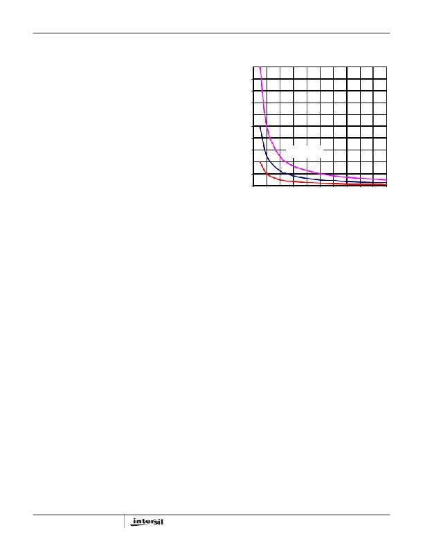
�capacitor� can� be� chosen� from� the� following� equation:�
�Q� GATE�
�Δ� V� BOOT�
�where� Q� GATE� is� the� amount� of� gate� charge� required� to� fully�
�charge� the� gate� of� the� upper� MOSFET.� The� Δ� V� BOOT� term� is�
�defined� as� the� allowable� droop� in� the� rail� of� the� upper� drive.�
�The� above� relationship� is� illustrated� in� Figure� 1.�
�As� an� example,� suppose� an� upper� MOSFET� has� a� gate�
�charge,� Q� GATE� ,� of� 65nC� at� 5V� and� also� assume� the� droop� in�
�the� drive� voltage� over� a� PWM� cycle� is� 200mV.� One� will� find�
�that� a� bootstrap� capacitance� of� at� least� 0.125� μ� F� is� required.�
�6�
�The� next� larger� standard� value� capacitance� is� 0.15� μ� F.� A�
�good� quality� ceramic� capacitor� is� recommended.�
�2.0�
�1.8�
�1.6�
�1.4�
�1.2�
�1.0�
�0.8�
�0.8�
�0.6�
�0.6�
�0.4�
�0.4�
�0.2�
�0.0�
�0.0� 0.0� 0.1� 0.2� 0.3� 0.4� 0.5� 0.6� 0.7� 0.8� 0.9� 1.0�
�0.0� 0.1� 0.2� 0.3� 0.4� 0.5� 0.6� 0.7� 0.8� 0.9� 1.0�
�Δ� V� BOOT� (V)�
�FIGURE� 1.� BOOTSTRAP� CAPACITANCE� vs.� BOOT� RIPPLE�
�VOLTAGE�
�Power� Dissipation�
�Package� power� dissipation� is� mainly� a� function� of� the�
�switching� frequency� and� total� gate� charge� of� the� selected�
�MOSFETs.� Calculating� the� power� dissipation� in� the� driver� for�
�a� desired� application� is� critical� to� ensuring� safe� operation.�
�Exceeding� the� maximum� allowable� power� dissipation� level�
�will� push� the� IC� beyond� the� maximum� recommended�
�operating� junction� temperature� of� 125°C.� The� maximum�
�allowable� IC� power� dissipation� for� the� SO-8� package� is�
�approximately� 800mW.� When� designing� the� driver� into� an�
�application,� it� is� recommended� that� the� following� calculation�
�be� performed� to� ensure� safe� operation� at� the� desired�
�frequency� for� the� selected� MOSFETs.� The� power� dissipated�
�by� the� driver� is� approximated� as� below� and� plotted� as� in�
�Figure� 2.�
�P� =� f� sw� (� 1.5V� U� Q� U� +� V� L� Q� L� )� +� I� DDQ� V� CC�
�where� f� sw� is� the� switching� frequency� of� the� PWM� signal.� V� U�
�and� V� L� represent� the� upper� and� lower� gate� rail� voltage.� Q� U�
�and� Q� L� are� the� upper� and� lower� gate� charge� determined� by�
�MOSFET� selection� and� any� external� capacitance� added� to�
�the� gate� pins.� The� I� DDQ� V� CC� product� is� the� quiescent� power�
�of� the� driver� and� is� typically� negligible.�
�FN9091.7�
�May� 9,� 2006�
�相关PDF资料 |
PDF描述 |
|---|---|
| VE-BNW-EV-B1 | CONVERTER MOD DC/DC 5.5V 150W |
| MBRD640CTG | DIODE SCHOTTKY 40V 3A DPAK |
| VE-BNW-EU-F4 | CONVERTER MOD DC/DC 5.5V 200W |
| MBRB30H60CTT4G | DIODE SCHOTTKY 60V 15A H D2PAK |
| GEC10DRTS-S734 | CONN EDGECARD 20POS DIP .100 SLD |
相关代理商/技术参数 |
参数描述 |
|---|---|
| ISL6605CRZ-TK | 功能描述:IC MOSFET DVR SYNC BUCK 8QFN RoHS:是 类别:集成电路 (IC) >> PMIC - MOSFET,电桥驱动器 - 外部开关 系列:- 标准包装:6,000 系列:* |
| ISL6605IB | 功能描述:功率驱动器IC MOSFET DUAL SYNC RoHS:否 制造商:Micrel 产品:MOSFET Gate Drivers 类型:Low Cost High or Low Side MOSFET Driver 上升时间: 下降时间: 电源电压-最大:30 V 电源电压-最小:2.75 V 电源电流: 最大功率耗散: 最大工作温度:+ 85 C 安装风格:SMD/SMT 封装 / 箱体:SOIC-8 封装:Tube |
| ISL6605IB-T | 功能描述:IC MOSFET DRVR SYNC BUCK 8-SOIC RoHS:否 类别:集成电路 (IC) >> PMIC - MOSFET,电桥驱动器 - 外部开关 系列:- 标准包装:50 系列:- 配置:低端 输入类型:非反相 延迟时间:40ns 电流 - 峰:9A 配置数:1 输出数:1 高端电压 - 最大(自引导启动):- 电源电压:4.5 V ~ 35 V 工作温度:-40°C ~ 125°C 安装类型:表面贴装 封装/外壳:TO-263-6,D²Pak(5 引线+接片),TO-263BA 供应商设备封装:TO-263 包装:管件 |
| ISL6605IBZ | 功能描述:IC DRIVER MOSFET DUAL SYNC 8SOIC RoHS:是 类别:集成电路 (IC) >> PMIC - MOSFET,电桥驱动器 - 外部开关 系列:- 标准包装:95 系列:- 配置:半桥 输入类型:PWM 延迟时间:25ns 电流 - 峰:1.6A 配置数:1 输出数:2 高端电压 - 最大(自引导启动):118V 电源电压:9 V ~ 14 V 工作温度:-40°C ~ 125°C 安装类型:表面贴装 封装/外壳:8-SOIC(0.154",3.90mm 宽) 供应商设备封装:8-SOIC 包装:管件 产品目录页面:1282 (CN2011-ZH PDF) 其它名称:*LM5104M*LM5104M/NOPBLM5104M |
| ISL6605IBZ-T | 功能描述:IC MOSFET DRVR SYNC BUCK 8-SOIC RoHS:是 类别:集成电路 (IC) >> PMIC - MOSFET,电桥驱动器 - 外部开关 系列:- 标准包装:5 系列:- 配置:低端 输入类型:非反相 延迟时间:600ns 电流 - 峰:12A 配置数:1 输出数:1 高端电压 - 最大(自引导启动):- 电源电压:14.2 V ~ 15.8 V 工作温度:-20°C ~ 60°C 安装类型:通孔 封装/外壳:21-SIP 模块 供应商设备封装:模块 包装:散装 配用:BG2A-NF-ND - KIT DEV BOARD FOR IGBT 其它名称:835-1063 |
发布紧急采购,3分钟左右您将得到回复。