- 您现在的位置:买卖IC网 > Datasheet目录334 > ISL6609AIRZ-TK (Intersil)IC MOSFET DVR SYNC RECT 8-QFN Datasheet资料下载
参数资料
| 型号: | ISL6609AIRZ-TK |
| 厂商: | Intersil |
| 文件页数: | 6/12页 |
| 文件大小: | 0K |
| 描述: | IC MOSFET DVR SYNC RECT 8-QFN |
| 标准包装: | 1 |
| 配置: | 高端和低端,同步 |
| 输入类型: | PWM |
| 延迟时间: | 18ns |
| 电流 - 峰: | 2A |
| 配置数: | 1 |
| 输出数: | 2 |
| 高端电压 - 最大(自引导启动): | 36V |
| 电源电压: | 4.5 V ~ 5.5 V |
| 工作温度: | -40°C ~ 85°C |
| 安装类型: | 表面贴装 |
| 封装/外壳: | 8-VQFN 裸露焊盘 |
| 供应商设备封装: | 8-QFN(3x3) |
| 包装: | 标准包装 |
| 产品目录页面: | 1248 (CN2011-ZH PDF) |
| 其它名称: | ISL6609AIRZ-TKDKR |
�� �
�
�ISL6609,� ISL6609A�
�Electrical� Specifications�
�These� specifications� apply� for� T� A� =� -40°C� to� 100°C,� unless� otherwise� noted.� Parameters� with� MIN� and/or� MAX�
�limits� are� 100%� tested� at� +25°C,� unless� otherwise� specified.� Temperature� limits� established� by� characterization�
�and� are� not� production� tested.� (Continued)�
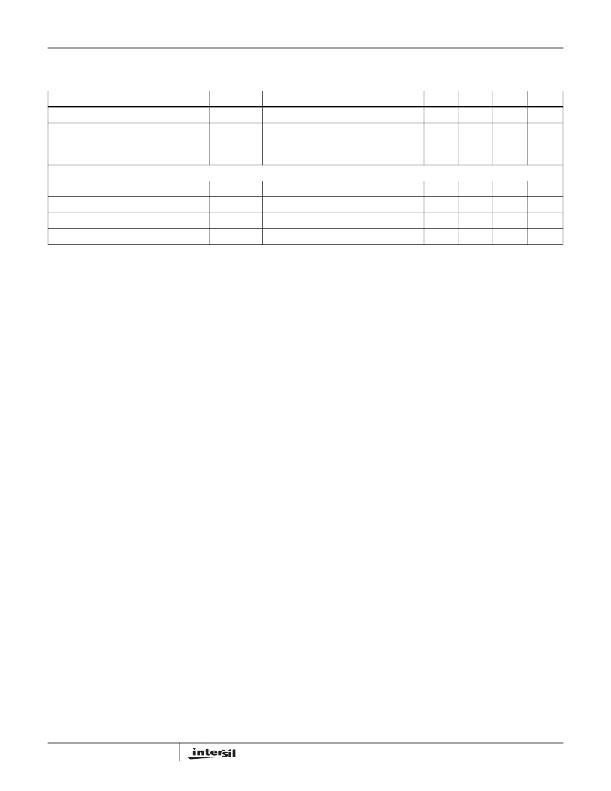
�PARAMETER�
�UGATE� Turn-On� Propagation� Delay�
�LGATE� Turn-On� Propagation� Delay�
�Three-state� to� UG/LG� Rising� Propagation�
�SYMBOL�
�t� PDHU�
�t� PDHL�
�t� PTS�
�TEST� CONDITIONS�
�V� VCC� =� 5V,� Outputs� Unloaded�
�V� VCC� =� 5V,� Outputs� Unloaded�
�V� VCC� =� 5V,� Outputs� Unloaded�
�MIN�
�-�
�-�
�-�
�TYP�
�18�
�23�
�20�
�MAX�
�-�
�-�
�-�
�UNITS�
�ns�
�ns�
�ns�
�Delay�
�OUTPUT�
�Upper� Drive� Source� Resistance�
�Upper� Drive� Sink� Resistance�
�Lower� Drive� Source� Resistance�
�Lower� Drive� Sink� Resistance�
�R� UG_SRC�
�R� UG_SNK�
�R� LG_SRC�
�R� LG_SNK�
�250mA� Source� Current�
�250mA� Sink� Current�
�250mA� Source� Current�
�250mA� Sink� Current�
�-�
�-�
�-�
�-�
�1.0�
�1.0�
�1.0�
�0.4�
�2.5�
�2.5�
�2.5�
�1.0�
�Ω�
�Ω�
�Ω�
�Ω�
�NOTE:�
�4.� Limits� established� by� characterization� and� are� not� production� tested�
�Functional� Pin� Description�
�Note:� Pin� numbers� refer� to� the� SOIC� package.� Check�
�diagram� for� corresponding� QFN� pinout.�
�UGATE� (Pin� 1)�
�Upper� gate� drive� output.� Connect� to� gate� of� high-side�
�N-Channel� power� MOSFET.� A� gate� resistor� is� never�
�recommended� on� this� pin,� as� it� interferes� with� the� operation�
�shoot-through� protection� circuitry.�
�BOOT� (Pin� 2)�
�Floating� bootstrap� supply� pin� for� the� upper� gate� drive.�
�Connect� a� bootstrap� capacitor� between� this� pin� and� the�
�PHASE� pin.� The� bootstrap� capacitor� provides� the� charge�
�used� to� turn� on� the� upper� MOSFET.� See� “Bootstrap�
�Considerations”� on� page� 7� for� guidance� in� choosing� the�
�appropriate� capacitor� value.�
�PWM� (Pin� 3)�
�The� PWM� signal� is� the� control� input� for� the� driver.� The� PWM�
�signal� can� enter� three� distinct� states� during� operation,� see�
�“Three-State� PWM� Input”� on� page� 7� for� further� details.� Connect�
�this� pin� to� the� PWM� output� of� the� controller.�
�GND� (Pin� 4)�
�Ground� pin.� All� signals� are� referenced� to� this� node.�
�6�
�LGATE� (Pin� 5)�
�Lower� gate� drive� output.� Connect� to� gate� of� the� low� side�
�N-Channel� power� MOSFET.� A� gate� resistor� is� never�
�recommended� on� this� pin,� as� it� interferes� with� the� operation�
�shoot-through� protection� circuitry.�
�VCC� (Pin� 6)�
�Connect� this� pin� to� a� +5V� bias� supply.� Locally� bypass� with� a�
�high� quality� ceramic� capacitor� to� ground.�
�EN� (Pin� 7)�
�Enable� input� pin.� Connect� this� pin� high� to� enable� and� low� to�
�disable� the� driver.�
�PHASE� (Pin� 8)�
�Connect� this� pin� to� the� source� of� the� upper� MOSFET.� This�
�pin� provides� the� return� path� for� the� upper� gate� driver� current.�
�Thermal� Pad� (in� QFN� only)�
�The� metal� pad� underneath� the� center� of� the� IC� is� a� thermal�
�substrate.� The� PCB� “thermal� land”� design� for� this� exposed�
�die� pad� should� include� vias� that� drop� down� and� connect� to�
�one� or� more� buried� copper� plane(s).� This� combination� of�
�vias� for� vertical� heat� escape� and� buried� planes� for� heat�
�spreading� allows� the� QFN� to� achieve� its� full� thermal�
�potential.� This� pad� should� be� either� grounded� or� floating,�
�and� it� should� not� be� connected� to� other� nodes.� Refer� to�
�TB389� for� design� guidelines.�
�FN9221.2�
�April� 27,� 2009�
�相关PDF资料 |
PDF描述 |
|---|---|
| ISL6610IRZ | IC MOSFET DRVR DUAL SYNC 16-QFN |
| ISL6612ACBZ | IC DRIVER MOSFET SYNC BUCK 8SOIC |
| ISL6612BCBZ | IC DRIVER MOSFET SYNC BUCK 8SOIC |
| ISL6613IR-T | IC MOSFET DRVR SYNC BUCK 10-DFN |
| ISL6614AIR-T | IC DRIVER DUAL SYNC BUCK 16-QFN |
相关代理商/技术参数 |
参数描述 |
|---|---|
| ISL6609CBZ | 功能描述:IC MOSFET DRVR SYNC BUCK 8-SOIC RoHS:是 类别:集成电路 (IC) >> PMIC - MOSFET,电桥驱动器 - 外部开关 系列:- 标准包装:5 系列:- 配置:低端 输入类型:非反相 延迟时间:600ns 电流 - 峰:12A 配置数:1 输出数:1 高端电压 - 最大(自引导启动):- 电源电压:14.2 V ~ 15.8 V 工作温度:-20°C ~ 60°C 安装类型:通孔 封装/外壳:21-SIP 模块 供应商设备封装:模块 包装:散装 配用:BG2A-NF-ND - KIT DEV BOARD FOR IGBT 其它名称:835-1063 |
| ISL6609CBZ-T | 功能描述:IC MOSFET DRVR SYNC BUCK 8-SOIC RoHS:是 类别:集成电路 (IC) >> PMIC - MOSFET,电桥驱动器 - 外部开关 系列:- 标准包装:5 系列:- 配置:低端 输入类型:非反相 延迟时间:600ns 电流 - 峰:12A 配置数:1 输出数:1 高端电压 - 最大(自引导启动):- 电源电压:14.2 V ~ 15.8 V 工作温度:-20°C ~ 60°C 安装类型:通孔 封装/外壳:21-SIP 模块 供应商设备封装:模块 包装:散装 配用:BG2A-NF-ND - KIT DEV BOARD FOR IGBT 其它名称:835-1063 |
| ISL6609CRZ | 功能描述:IC MOSFET DRVR SYNC BUCK 8-QFN RoHS:是 类别:集成电路 (IC) >> PMIC - MOSFET,电桥驱动器 - 外部开关 系列:- 标准包装:5 系列:- 配置:低端 输入类型:非反相 延迟时间:600ns 电流 - 峰:12A 配置数:1 输出数:1 高端电压 - 最大(自引导启动):- 电源电压:14.2 V ~ 15.8 V 工作温度:-20°C ~ 60°C 安装类型:通孔 封装/外壳:21-SIP 模块 供应商设备封装:模块 包装:散装 配用:BG2A-NF-ND - KIT DEV BOARD FOR IGBT 其它名称:835-1063 |
| ISL6609CRZ-T | 功能描述:IC MOSFET DRVR SYNC BUCK 8-QFN RoHS:是 类别:集成电路 (IC) >> PMIC - MOSFET,电桥驱动器 - 外部开关 系列:- 标准包装:5 系列:- 配置:低端 输入类型:非反相 延迟时间:600ns 电流 - 峰:12A 配置数:1 输出数:1 高端电压 - 最大(自引导启动):- 电源电压:14.2 V ~ 15.8 V 工作温度:-20°C ~ 60°C 安装类型:通孔 封装/外壳:21-SIP 模块 供应商设备封装:模块 包装:散装 配用:BG2A-NF-ND - KIT DEV BOARD FOR IGBT 其它名称:835-1063 |
| ISL6609IBZ | 功能描述:IC MOSFET DRVR SYNC BUCK 8-SOIC RoHS:是 类别:集成电路 (IC) >> PMIC - MOSFET,电桥驱动器 - 外部开关 系列:- 标准包装:5 系列:- 配置:低端 输入类型:非反相 延迟时间:600ns 电流 - 峰:12A 配置数:1 输出数:1 高端电压 - 最大(自引导启动):- 电源电压:14.2 V ~ 15.8 V 工作温度:-20°C ~ 60°C 安装类型:通孔 封装/外壳:21-SIP 模块 供应商设备封装:模块 包装:散装 配用:BG2A-NF-ND - KIT DEV BOARD FOR IGBT 其它名称:835-1063 |
发布紧急采购,3分钟左右您将得到回复。