- 您现在的位置:买卖IC网 > Datasheet目录334 > ISL6609AIRZ-TK (Intersil)IC MOSFET DVR SYNC RECT 8-QFN Datasheet资料下载
参数资料
| 型号: | ISL6609AIRZ-TK |
| 厂商: | Intersil |
| 文件页数: | 8/12页 |
| 文件大小: | 0K |
| 描述: | IC MOSFET DVR SYNC RECT 8-QFN |
| 标准包装: | 1 |
| 配置: | 高端和低端,同步 |
| 输入类型: | PWM |
| 延迟时间: | 18ns |
| 电流 - 峰: | 2A |
| 配置数: | 1 |
| 输出数: | 2 |
| 高端电压 - 最大(自引导启动): | 36V |
| 电源电压: | 4.5 V ~ 5.5 V |
| 工作温度: | -40°C ~ 85°C |
| 安装类型: | 表面贴装 |
| 封装/外壳: | 8-VQFN 裸露焊盘 |
| 供应商设备封装: | 8-QFN(3x3) |
| 包装: | 标准包装 |
| 产品目录页面: | 1248 (CN2011-ZH PDF) |
| 其它名称: | ISL6609AIRZ-TKDKR |
�� �
�
�ISL6609,� ISL6609A�
�bootstrap� resistor� is� designed� to� reduce� the� overcharging� of�
�the� bootstrap� capacitor� when� exposed� to� excessively� large�
�negative� voltage� swing� at� the� PHASE� node.� Typically,� such�
�large� negative� excursions� occur� in� high� current� applications�
�that� use� D� 2� -PAK� and� D-PAK� MOSFETs� or� excessive� layout�
�parasitic� inductance.�
�The� following� equation� helps� select� a� proper� bootstrap�
�capacitor� size:�
�allowable� power� dissipation� level� will� push� the� IC� beyond� the�
�maximum� recommended� operating� junction� temperature� of�
�+125°C.� The� maximum� allowable� IC� power� dissipation� for�
�the� SO8� package� is� approximately� 800mW� at� room�
�temperature,� while� the� power� dissipation� capacity� in� the�
�QFN� package,� with� an� exposed� heat� escape� pad,� is� slightly�
�better.� See� “Layout� Considerations”� on� page� 9� for� thermal�
�transfer� improvement� suggestions.� When� designing� the�
�driver� into� an� application,� it� is� recommended� that� the�
�C� BOOT_CAP� ≥� --------------------------------------�
�Q� GATE� =� -------------------------------� ?� N� Q1�
�Q� GATE�
�Δ� V� BOOT_CAP�
�Q� G1� ?� VCC�
�V� GS1�
�(EQ.� 1)�
�following� calculation� is� used� to� ensure� safe� operation� at� the�
�desired� frequency� for� the� selected� MOSFETs.� The� total� gate�
�drive� power� losses� due� to� the� gate� charge� of� MOSFETs� and�
�the� driver� ’s� internal� circuitry� and� their� corresponding� average�
�driver� current� can� be� estimated� with� Equations� 2� and� 3,�
�respectively,�
�P� Qg_Q1� =� ----------------------------------� ?� F� SW� ?� N� Q1�
�P� Qg_Q2� =� ----------------------------------� ?� F� SW� ?� N� Q2�
�where� Q� G1� is� the� amount� of� gate� charge� per� upper� MOSFET�
�at� V� GS1� gate-source� voltage� and� N� Q1� is� the� number� of�
�control� MOSFETs.� The� Δ� V� BOOT_CAP� term� is� defined� as� the�
�allowable� droop� in� the� rail� of� the� upper� gate� drive.�
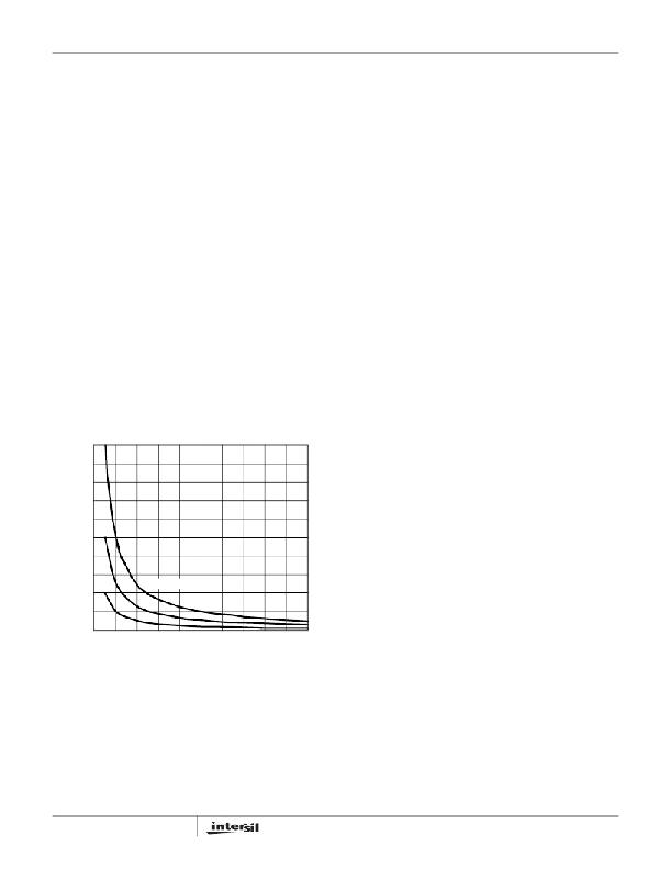
�As� an� example,� suppose� two� IRLR7821� FETs� are� chosen� as�
�the� upper� MOSFETs.� The� gate� charge,� Q� G� ,� from� the� data�
�sheet� is� 10nC� at� 4.5V� (V� GS� )� gate-source� voltage.� Then� the�
�Q� GATE� is� calculated� to� be� 22nC� at� VCC� level.� We� will�
�P� Qg_TOT� =� P� Qg_Q1� +� P� Qg_Q2� +� I� Q� ?� VCC�
�Q� G1� ?� VCC� 2�
�V� GS1�
�Q� G2� ?� VCC� 2�
�V� GS2�
�(EQ.� 2)�
�I� DR� =� ?� ------------------------------------------------------� +� -----------------------------------------------------� ?� ?� F� SW� +� I� Q�
�assume� a� 200mV� droop� in� drive� voltage� over� the� PWM�
�cycle.� We� find� that� a� bootstrap� capacitance� of� at� least�
�0.110μF� is� required.� The� next� larger� standard� value�
�capacitance� is� 0.22μF.� A� good� quality� ceramic� capacitor� is�
�recommended.�
�2.0�
�1.8�
�1.6�
�1.4�
�1.2�
�1.0�
�0.8�
�0.6�
�?� Q� G1� ?� UVCC� ?� N� Q1� Q� G2� ?� LVCC� ?� N� Q2� ?�
�?� V� GS1� V� GS2� ?�
�(EQ.� 3)�
�where� the� gate� charge� (Q� G1� and� Q� G2� )� is� defined� at� a�
�particular� gate� to� source� voltage� (V� GS1� and� V� GS2� )� in� the�
�corresponding� MOSFET� datasheet;� I� Q� is� the� driver� ’s� total�
�quiescent� current� with� no� load� at� both� drive� outputs;� N� Q1�
�and� N� Q2� are� number� of� upper� and� lower� MOSFETs,�
�respectively.� The� I� Q� V� CC� product� is� the� quiescent� power� of�
�the� driver� without� capacitive� load� and� is� typically� negligible.�
�The� total� gate� drive� power� losses� are� dissipated� among� the�
�resistive� components� along� the� transition� path.� The� drive�
�resistance� dissipates� a� portion� of� the� total� gate� drive� power�
�losses,� the� rest� will� be� dissipated� by� the� external� gate�
�0.4�
�0.2�
�20nC�
�0.0�
�0.0� 0.1�
�Q� GATE� = 100nC�
�50nC�
�0.2� 0.3� 0.4� 0.5�
�0.6�
�0.7�
�0.8�
�0.9�
�1.0�
�resistors� (R� G1� and� R� G2� ,� should� be� a� short� to� avoid�
�interfering� with� the� operation� shoot-through� protection�
�circuitry)� and� the� internal� gate� resistors� (R� GI1� and� R� GI2� )� of�
�MOSFETs.� Figures� 3� and� 4� show� the� typical� upper� and� lower�
�gate� drives� turn-on� transition� path.� The� power� dissipation� on�
�Δ� V� BOOT� (V)�
�FIGURE� 2.� BOOTSTRAP� CAPACITANCE� vs� BOOT� RIPPLE�
�the� driver� can� be� roughly� estimated� as:�
�P� DR_UP� =� ?� --------------------------------------� +� ----------------------------------------� ?� ?� ---------------------�
�?� R� HI1� +� R� EXT1� R� LO1� +� R� EXT1� ?�
�P� DR_LOW� =� ?� ?� ?� ---------------------�
�?� R� HI2� +� R� EXT2� R� LO2� +� R� EXT2� ?�
�VOLTAGE�
�Power� Dissipation�
�Package� power� dissipation� is� mainly� a� function� of� the�
�switching� frequency� (F� SW� ),� the� output� drive� impedance,� the�
�external� gate� resistance,� and� the� selected� MOSFET’s�
�internal� gate� resistance� and� total� gate� charge.� Calculating�
�P� DR� =� P� DR_UP� +� P� DR_LOW� +� I� Q� ?� VCC�
�?� R� HI1� R� LO1� ?� P� Qg_Q1�
�?� R� HI2� R� LO2� ?� P� Qg_Q2�
�--------------------------------------� +� ----------------------------------------�
�2�
�2�
�(EQ.� 4)�
�R� EXT2� =� R� G1� +� -------------�
�N�
�R� EXT2� =� R� G2� +� -------------�
�N�
�the� power� dissipation� in� the� driver� for� a� desired� application� is�
�critical� to� ensure� safe� operation.� Exceeding� the� maximum�
�8�
�R� GI1�
�Q1�
�R� GI2�
�Q2�
�FN9221.2�
�April� 27,� 2009�
�相关PDF资料 |
PDF描述 |
|---|---|
| ISL6610IRZ | IC MOSFET DRVR DUAL SYNC 16-QFN |
| ISL6612ACBZ | IC DRIVER MOSFET SYNC BUCK 8SOIC |
| ISL6612BCBZ | IC DRIVER MOSFET SYNC BUCK 8SOIC |
| ISL6613IR-T | IC MOSFET DRVR SYNC BUCK 10-DFN |
| ISL6614AIR-T | IC DRIVER DUAL SYNC BUCK 16-QFN |
相关代理商/技术参数 |
参数描述 |
|---|---|
| ISL6609CBZ | 功能描述:IC MOSFET DRVR SYNC BUCK 8-SOIC RoHS:是 类别:集成电路 (IC) >> PMIC - MOSFET,电桥驱动器 - 外部开关 系列:- 标准包装:5 系列:- 配置:低端 输入类型:非反相 延迟时间:600ns 电流 - 峰:12A 配置数:1 输出数:1 高端电压 - 最大(自引导启动):- 电源电压:14.2 V ~ 15.8 V 工作温度:-20°C ~ 60°C 安装类型:通孔 封装/外壳:21-SIP 模块 供应商设备封装:模块 包装:散装 配用:BG2A-NF-ND - KIT DEV BOARD FOR IGBT 其它名称:835-1063 |
| ISL6609CBZ-T | 功能描述:IC MOSFET DRVR SYNC BUCK 8-SOIC RoHS:是 类别:集成电路 (IC) >> PMIC - MOSFET,电桥驱动器 - 外部开关 系列:- 标准包装:5 系列:- 配置:低端 输入类型:非反相 延迟时间:600ns 电流 - 峰:12A 配置数:1 输出数:1 高端电压 - 最大(自引导启动):- 电源电压:14.2 V ~ 15.8 V 工作温度:-20°C ~ 60°C 安装类型:通孔 封装/外壳:21-SIP 模块 供应商设备封装:模块 包装:散装 配用:BG2A-NF-ND - KIT DEV BOARD FOR IGBT 其它名称:835-1063 |
| ISL6609CRZ | 功能描述:IC MOSFET DRVR SYNC BUCK 8-QFN RoHS:是 类别:集成电路 (IC) >> PMIC - MOSFET,电桥驱动器 - 外部开关 系列:- 标准包装:5 系列:- 配置:低端 输入类型:非反相 延迟时间:600ns 电流 - 峰:12A 配置数:1 输出数:1 高端电压 - 最大(自引导启动):- 电源电压:14.2 V ~ 15.8 V 工作温度:-20°C ~ 60°C 安装类型:通孔 封装/外壳:21-SIP 模块 供应商设备封装:模块 包装:散装 配用:BG2A-NF-ND - KIT DEV BOARD FOR IGBT 其它名称:835-1063 |
| ISL6609CRZ-T | 功能描述:IC MOSFET DRVR SYNC BUCK 8-QFN RoHS:是 类别:集成电路 (IC) >> PMIC - MOSFET,电桥驱动器 - 外部开关 系列:- 标准包装:5 系列:- 配置:低端 输入类型:非反相 延迟时间:600ns 电流 - 峰:12A 配置数:1 输出数:1 高端电压 - 最大(自引导启动):- 电源电压:14.2 V ~ 15.8 V 工作温度:-20°C ~ 60°C 安装类型:通孔 封装/外壳:21-SIP 模块 供应商设备封装:模块 包装:散装 配用:BG2A-NF-ND - KIT DEV BOARD FOR IGBT 其它名称:835-1063 |
| ISL6609IBZ | 功能描述:IC MOSFET DRVR SYNC BUCK 8-SOIC RoHS:是 类别:集成电路 (IC) >> PMIC - MOSFET,电桥驱动器 - 外部开关 系列:- 标准包装:5 系列:- 配置:低端 输入类型:非反相 延迟时间:600ns 电流 - 峰:12A 配置数:1 输出数:1 高端电压 - 最大(自引导启动):- 电源电压:14.2 V ~ 15.8 V 工作温度:-20°C ~ 60°C 安装类型:通孔 封装/外壳:21-SIP 模块 供应商设备封装:模块 包装:散装 配用:BG2A-NF-ND - KIT DEV BOARD FOR IGBT 其它名称:835-1063 |
发布紧急采购,3分钟左右您将得到回复。