- 您现在的位置:买卖IC网 > PDF目录15211 > ISL8105BCBZ (Intersil)IC REG CTRLR BUCK PWM VM 8-SOIC PDF资料下载
参数资料
| 型号: | ISL8105BCBZ |
| 厂商: | Intersil |
| 文件页数: | 10/16页 |
| 文件大小: | 0K |
| 描述: | IC REG CTRLR BUCK PWM VM 8-SOIC |
| 标准包装: | 980 |
| PWM 型: | 电压模式 |
| 输出数: | 1 |
| 频率 - 最大: | 330kHz |
| 占空比: | 100% |
| 电源电压: | 6.5 V ~ 14.4 V |
| 降压: | 是 |
| 升压: | 无 |
| 回扫: | 无 |
| 反相: | 无 |
| 倍增器: | 无 |
| 除法器: | 无 |
| Cuk: | 无 |
| 隔离: | 无 |
| 工作温度: | 0°C ~ 70°C |
| 封装/外壳: | 8-SOIC(0.154",3.90mm 宽) |
| 包装: | 管件 |
�� �
�
�ISL8105B�
�Another� consideration� for� high� V� IN� is� duty� cycle.� Very� low�
�duty� cycles� (such� as� 20V� in� to� 1.0V� out,� for� 5%� duty� cycle)�
�require� component� selection� compatible� with� that� choice�
�(such� as� low� r� DS(ON)� bottom-side� MOSFET,� and� a� good� LC�
�output� filter).� At� the� other� extreme� (for� example,� 20V� in� to�
�ISL8105B�
�V� IN�
�12V� out),� the� top-side� MOSFET� needs� to� be� low� r� DS(ON)� .� In�
�addition,� if� the� duty� cycle� gets� too� high,� it� can� affect� the�
�overcurrent� sample� time.� In� all� cases,� the� input� and� output�
�capacitors� and� both� MOSFETs� must� be� rated� for� the�
�voltages� present.�
�TGATE�
�LX�
�BGATE�
�Q� 1�
�Q� 2�
�C� IN�
�L� O�
�C� O�
�V� OUT�
�+V� IN�
�BOOT� Refresh�
�In� the� event� that� the� TGATE� is� on� for� an� extended� period� of�
�time,� the� charge� on� the� boot� capacitor� can� start� to� sag,�
�raising� the� r� DS(ON)� of� the� top-side� MOSFET.� The� ISL8105B�
�has� a� circuit� that� detects� a� long� TGATE� on-time� (nominal�
�100μs),� and� forces� the� BGATE� to� go� high� for� one� clock�
�cycle,� which� will� allow� the� boot� capacitor� some� time� to�
�recharge.� Separately,� the� OCP� circuit� has� a� BGATE� pulse�
�stretcher� (to� be� sure� the� sample� time� is� long� enough),� which�
�can� also� help� refresh� the� boot.� But� if� OCP� is� disabled� (no�
�current� sense� resistor),� the� regular� boot� refresh� circuit� will�
�still� be� active.�
�Current� Sinking�
�The� ISL8105B� incorporates� a� MOSFET� shoot-through�
�protection� method� which� allows� a� converter� to� sink� current�
�as� well� as� source� current.� Care� should� be� exercised� when�
�designing� a� converter� with� the� ISL8105B� when� it� is� known�
�that� the� converter� may� sink� current.�
�When� the� converter� is� sinking� current,� it� is� behaving� as� a�
�boost� converter� that� is� regulating� its� input� voltage.� This�
�means� that� the� converter� is� boosting� current� into� the� V� IN� rail.�
�If� there� is� nowhere� for� this� current� to� go,� such� as� to� other�
�distributed� loads� on� the� V� IN� rail,� through� a� voltage� limiting�
�protection� device,� or� other� methods,� the� capacitance� on� the�
�PGND�
�RETURN�
�FIGURE� 7.� PRINTED� CIRCUIT� BOARD� POWER� AND�
�GROUND� PLANES� OR� ISLANDS�
�Figure� 7� shows� the� critical� power� components� of� the�
�converter.� To� minimize� the� voltage� overshoot/undershoot,�
�the� interconnecting� wires� indicated� by� heavy� lines� should� be�
�part� of� ground� or� power� plane� in� a� printed� circuit� board.� The�
�components� shown� in� Figure� 8� should� be� located� as� close�
�together� as� possible.� Please� note� that� the� capacitors� C� IN�
�and� C� O� each� represent� numerous� physical� capacitors.�
�Locate� the� ISL8105B� within� three� inches� of� the� MOSFETs,�
�Q� 1� and� Q� 2� .� The� circuit� traces� for� the� MOSFETs’� gate� and�
�source� connections� from� the� ISL8105B� must� be� sized� to�
�handle� up� to� 1A� peak� current.�
�Proper� grounding� of� the� IC� is� important� for� correct� operation�
�in� noisy� environments.� The� GND� pin� should� be� connected� to�
�a� large� copper� fill� under� the� IC� which� is� subsequently�
�connected� to� board� ground� at� a� quiet� location� on� the� board,�
�typically� found� at� an� input� or� output� bulk� (electrolytic)�
�capacitor.�
�BOOT�
�V� IN� bus� will� absorb� the� current.� This� situation� will� allow�
�voltage� level� of� the� V� IN� rail� (also� LX)� to� increase.� If� the�
�voltage� level� of� the� LX� is� increased� to� a� level� that� exceeds�
�ISL8105B�
�C� BOOT�
�LX�
�Q� 1�
�L� O�
�V� OUT�
�the� maximum� voltage� rating� of� the� ISL8105B,� then� the� IC� will�
�experience� an� irreversible� failure� and� the� converter� will� no�
�longer� be� operational.� Ensuring� that� there� is� a� path� for� the�
�current� to� follow� other� than� the� capacitance� on� the� rail� will�
�prevent� this� failure� mode.�
�+V� BIAS�
�BGATE/BSOC�
�V� BIAS�
�C� VBIAS�
�GND� GND�
�Q� 2�
�C� O�
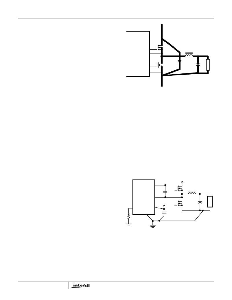
�Application� Guidelines�
�Layout� Considerations�
�As� in� any� high-frequency� switching� converter,� layout� is� very�
�important.� Switching� current� from� one� power� device� to� another�
�can� generate� voltage� transients� across� the� impedances� of� the�
�interconnecting� bond� wires� and� circuit� traces.� These�
�interconnecting� impedances� should� be� minimized� by� using�
�wide,� short� printed� circuit� traces.� The� critical� components�
�should� be� located� as� close� together� as� possible� using� ground�
�plane� construction� or� single� point� grounding.�
�10�
�FIGURE� 8.� PRINTED� CIRCUIT� BOARD� SMALL� SIGNAL�
�LAYOUT� GUIDELINES�
�Figure� 8� shows� the� circuit� traces� that� require� additional�
�layout� consideration.� Use� single� point� and� ground� plane�
�construction� for� the� circuits� shown.� Locate� the� resistor,�
�R� BSOC� ,� close� to� the� BGATE/BSOC� pin� as� the� internal� BSOC�
�current� source� is� only� 21.5μA.� Minimize� the� loop� from� any�
�pulldown� transistor� to� reduce� antenna� effect.� Provide� local�
�decoupling� between� VBIAS� and� GND� pins� as� described�
�FN6447.2�
�April� 15,� 2010�
�相关PDF资料 |
PDF描述 |
|---|---|
| VI-B7Y-EW-F3 | CONVERTER MOD DC/DC 3.3V 66W |
| ISL8105BCRZ | IC REG CTRLR BUCK PWM VM 10-DFN |
| CAT823LTDI-GT3 | IC SUPERVISOR RESET TSOT-23-5 |
| ISL8105ACRZ | IC REG CTRLR BUCK PWM VM 10-DFN |
| ISL8105CRZ | IC REG CTRLR BUCK PWM VM 10-DFN |
相关代理商/技术参数 |
参数描述 |
|---|---|
| ISL8105BCBZ-T | 功能描述:IC REG CTRLR BUCK PWM VM 8-SOIC RoHS:是 类别:集成电路 (IC) >> PMIC - 稳压器 - DC DC 切换控制器 系列:- 标准包装:4,500 系列:PowerWise® PWM 型:控制器 输出数:1 频率 - 最大:1MHz 占空比:95% 电源电压:2.8 V ~ 5.5 V 降压:是 升压:无 回扫:无 反相:无 倍增器:无 除法器:无 Cuk:无 隔离:无 工作温度:-40°C ~ 125°C 封装/外壳:6-WDFN 裸露焊盘 包装:带卷 (TR) 配用:LM1771EVAL-ND - BOARD EVALUATION LM1771 其它名称:LM1771SSDX |
| ISL8105BCRZ | 功能描述:IC REG CTRLR BUCK PWM VM 10-DFN RoHS:是 类别:集成电路 (IC) >> PMIC - 稳压器 - DC DC 切换控制器 系列:- 产品培训模块:Lead (SnPb) Finish for COTS Obsolescence Mitigation Program 标准包装:2,500 系列:- PWM 型:电流模式 输出数:1 频率 - 最大:275kHz 占空比:50% 电源电压:18 V ~ 110 V 降压:无 升压:无 回扫:无 反相:无 倍增器:无 除法器:无 Cuk:无 隔离:是 工作温度:-40°C ~ 85°C 封装/外壳:8-SOIC(0.154",3.90mm 宽) 包装:带卷 (TR) |
| ISL8105BCRZ-T | 功能描述:IC REG CTRLR BUCK PWM VM 10-DFN RoHS:是 类别:集成电路 (IC) >> PMIC - 稳压器 - DC DC 切换控制器 系列:- 标准包装:4,500 系列:PowerWise® PWM 型:控制器 输出数:1 频率 - 最大:1MHz 占空比:95% 电源电压:2.8 V ~ 5.5 V 降压:是 升压:无 回扫:无 反相:无 倍增器:无 除法器:无 Cuk:无 隔离:无 工作温度:-40°C ~ 125°C 封装/外壳:6-WDFN 裸露焊盘 包装:带卷 (TR) 配用:LM1771EVAL-ND - BOARD EVALUATION LM1771 其它名称:LM1771SSDX |
| ISL8105BEVAL1Z | 功能描述:EVAL BOARD ISL8105B RoHS:是 类别:编程器,开发系统 >> 评估板 - DC/DC 与 AC/DC(离线)SMPS 系列:- 产品培训模块:Obsolescence Mitigation Program 标准包装:1 系列:True Shutdown™ 主要目的:DC/DC,步升 输出及类型:1,非隔离 功率 - 输出:- 输出电压:- 电流 - 输出:1A 输入电压:2.5 V ~ 5.5 V 稳压器拓扑结构:升压 频率 - 开关:3MHz 板类型:完全填充 已供物品:板 已用 IC / 零件:MAX8969 |
| ISL8105BEVAL2Z | 功能描述:EVALUATION BOARD FOR ISL8105B RoHS:是 类别:编程器,开发系统 >> 评估板 - DC/DC 与 AC/DC(离线)SMPS 系列:- 产品培训模块:Obsolescence Mitigation Program 标准包装:1 系列:True Shutdown™ 主要目的:DC/DC,步升 输出及类型:1,非隔离 功率 - 输出:- 输出电压:- 电流 - 输出:1A 输入电压:2.5 V ~ 5.5 V 稳压器拓扑结构:升压 频率 - 开关:3MHz 板类型:完全填充 已供物品:板 已用 IC / 零件:MAX8969 |
发布紧急采购,3分钟左右您将得到回复。