- 您现在的位置:买卖IC网 > PDF目录15211 > ISL8105BCBZ (Intersil)IC REG CTRLR BUCK PWM VM 8-SOIC PDF资料下载
参数资料
| 型号: | ISL8105BCBZ |
| 厂商: | Intersil |
| 文件页数: | 6/16页 |
| 文件大小: | 0K |
| 描述: | IC REG CTRLR BUCK PWM VM 8-SOIC |
| 标准包装: | 980 |
| PWM 型: | 电压模式 |
| 输出数: | 1 |
| 频率 - 最大: | 330kHz |
| 占空比: | 100% |
| 电源电压: | 6.5 V ~ 14.4 V |
| 降压: | 是 |
| 升压: | 无 |
| 回扫: | 无 |
| 反相: | 无 |
| 倍增器: | 无 |
| 除法器: | 无 |
| Cuk: | 无 |
| 隔离: | 无 |
| 工作温度: | 0°C ~ 70°C |
| 封装/外壳: | 8-SOIC(0.154",3.90mm 宽) |
| 包装: | 管件 |
�� �
�
�ISL8105B�
�circuitry� to� determine� when� the� top-side� MOSFET� has� turned�
�off.�
�N/C� (DFN� Only;� Pin3,� Pin� 7)�
�These� two� pins� in� the� DFN� package� are� Not� Connected.�
�Functional� Description�
�COMP/EN�
�BGATE�
�STARTS�
�SWITCHING�
�Initialization� (POR� and� OCP� Sampling)�
�t0�
�BGATE/BSOC�
�V� OUT�
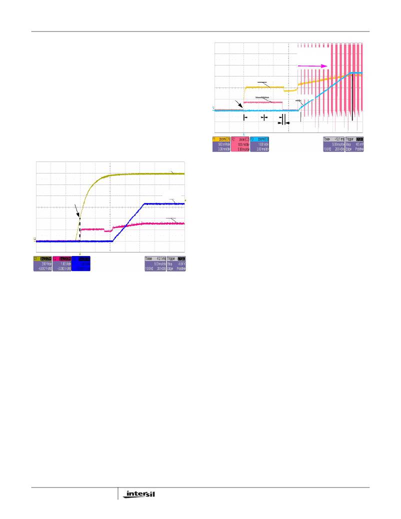
�Figure� 1� shows� a� start-up� waveform� of� ISL8105B.� The�
�Power-On-Reset� (POR)� function� continually� monitors� the�
�bias� voltage� at� the� VBIAS� pin.� Once� the� rising� POR�
�3.4ms�
�3.4ms�
�0ms� TO� 3.4ms�
�threshold� is� exceeded� 4V� (V� POR� nominal),� the� POR� function�
�initiates� the� Overcurrent� Protection� (OCP)� sample� and� hold�
�t1�
�t2� t3�
�t4�
�t5�
�operation� (while� COMP/EN� is� ~1V).� When� the� sampling� is�
�complete,� V� OUT� begins� the� soft-start� ramp.�
�V� BIAS�
�FIGURE� 2.� BGATE/BSOC� AND� SOFT-START� OPERATION�
�sample� and� hold� uses� a� digital� counter� and� DAC� to� save� the�
�voltage,� so� the� stored� value� does� not� degrade,� for� as� long� as�
�~4V� POR�
�V� OUT�
�V� COMP/EN�
�the� V� BIAS� is� above� V� POR� .� See� “Overcurrent� Protection�
��variables.� Upon� the� completion� of� sample� and� hold� at� t� 3� ,� the�
�soft-start� operation� is� initiated,� and� the� output� voltage� ramps�
�up� between� t� 4� and� t� 5� .�
�Soft-Start� and� Pre-Biased� Outputs�
�Functionally,� the� soft-start� internally� ramps� the� reference� on�
�the� non-inverting� terminal� of� the� error� amp� from� 0V� to� 0.6V� in�
�a� nominal� 13.6ms.� The� output� voltage� will� thus� follow� the�
�ramp,� from� zero� to� final� value,� in� the� same� 13.6ms� (the�
�FIGURE� 1.� POR� AND� SOFT-START� OPERATION�
�If� the� COMP/EN� pin� is� held� low� during� power-up,� the�
�initialization� will� be� delayed� until� the� COMP/EN� is� released�
�and� its� voltage� rises� above� the� V� DISABLE� trip� point.�
�Figure� 2� shows� a� typical� power-up� sequence� in� more� detail.�
�The� initialization� starts� at� t� 0� ,� when� either� V� BIAS� rises� above�
�V� POR� ,� or� the� COMP/EN� pin� is� released� (after� POR).� The�
�COMP/EN� will� be� pulled� up� by� an� internal� 20μA� current�
�source,� but� the� timing� will� not� begin� until� the� COMP/EN�
�exceeds� the� V� DISABLE� trip� point� (at� t� 1� ).� The� external�
�capacitance� of� the� disabling� device,� as� well� as� the�
�compensation� capacitors,� will� determine� how� quickly� the�
�20μA� current� source� will� charge� the� COMP/EN� pin.� With�
�typical� values,� it� should� add� a� small� delay� compared� to� the�
�soft-start� times.� The� COMP/EN� will� continue� to� ramp� to� ~1V.�
�From� t� 1� ,� there� is� a� nominal� 6.8ms� delay,� which� allows� the�
�VBIAS� pin� to� exceed� 6.5V� (if� rising� up� towards� 12V),� so� that�
�the� internal� bias� regulator� can� turn� on� cleanly.� At� the� same�
�time,� the� BGATE/BSOC� pin� is� initialized� by� disabling� the�
�BGATE� driver� and� drawing� BSOC� (nominal� 21.5μA)� through�
�R� BSOC� .� This� sets� up� a� voltage� that� will� represent� the� BSOC�
�trip� point.� At� t� 2� ,� there� is� a� variable� time� period� for� the� OCP�
�sample� and� hold� operation� (0ms� to� 3.4ms� nominal;� the�
�longer� time� occurs� with� the� higher� overcurrent� setting).� The�
�6�
�actual� ramp� seen� on� the� V� OUT� will� be� less� than� the� nominal�
�time),� due� to� some� initialization� timing,� between� t� 3� and� t� 4� ).�
�The� ramp� is� created� digitally,� so� there� will� be� 64� small�
�discrete� steps.� There� is� no� simple� way� to� change� this� ramp�
�rate� externally.�
�After� an� initialization� period� (t� 3� to� t� 4� ),� the� error� amplifier�
�(COMP/EN� pin)� is� enabled,� and� begins� to� regulate� the�
�converter's� output� voltage� during� soft-start.� The� oscillator's�
�triangular� waveform� is� compared� to� the� ramping� error�
�amplifier� voltage.� This� generates� LX� pulses� of� increasing�
�width� that� charge� the� output� capacitors.� When� the� internally�
�generated� soft-start� voltage� exceeds� the� reference� voltage�
�(0.6V),� the� soft-start� is� complete� and� the� output� should� be� in�
�regulation� at� the� expected� voltage.� This� method� provides� a�
�rapid� and� controlled� output� voltage� rise;� there� is� no� large�
�inrush� current� charging� the� output� capacitors.� The� entire�
�start-up� sequence� from� POR� typically� takes� up� to� 23.8ms;� up�
�to� 10.2ms� for� the� delay� and� OCP� sample� and� 13.6ms� for� the�
�soft-start� ramp.�
�Figure� 3� shows� the� normal� curve� in� yellow;� initialization�
�begins� at� t� 0� ,� and� the� output� ramps� between� t� 1� and� t� 2� .� If� the�
�output� is� pre-biased� to� a� voltage� less� than� the� expected�
�value,� as� shown� by� the� green� curve,� the� ISL8105B� will�
�detect� that� condition.� Neither� MOSFET� will� turn� on� until� the�
�FN6447.2�
�April� 15,� 2010�
�相关PDF资料 |
PDF描述 |
|---|---|
| VI-B7Y-EW-F3 | CONVERTER MOD DC/DC 3.3V 66W |
| ISL8105BCRZ | IC REG CTRLR BUCK PWM VM 10-DFN |
| CAT823LTDI-GT3 | IC SUPERVISOR RESET TSOT-23-5 |
| ISL8105ACRZ | IC REG CTRLR BUCK PWM VM 10-DFN |
| ISL8105CRZ | IC REG CTRLR BUCK PWM VM 10-DFN |
相关代理商/技术参数 |
参数描述 |
|---|---|
| ISL8105BCBZ-T | 功能描述:IC REG CTRLR BUCK PWM VM 8-SOIC RoHS:是 类别:集成电路 (IC) >> PMIC - 稳压器 - DC DC 切换控制器 系列:- 标准包装:4,500 系列:PowerWise® PWM 型:控制器 输出数:1 频率 - 最大:1MHz 占空比:95% 电源电压:2.8 V ~ 5.5 V 降压:是 升压:无 回扫:无 反相:无 倍增器:无 除法器:无 Cuk:无 隔离:无 工作温度:-40°C ~ 125°C 封装/外壳:6-WDFN 裸露焊盘 包装:带卷 (TR) 配用:LM1771EVAL-ND - BOARD EVALUATION LM1771 其它名称:LM1771SSDX |
| ISL8105BCRZ | 功能描述:IC REG CTRLR BUCK PWM VM 10-DFN RoHS:是 类别:集成电路 (IC) >> PMIC - 稳压器 - DC DC 切换控制器 系列:- 产品培训模块:Lead (SnPb) Finish for COTS Obsolescence Mitigation Program 标准包装:2,500 系列:- PWM 型:电流模式 输出数:1 频率 - 最大:275kHz 占空比:50% 电源电压:18 V ~ 110 V 降压:无 升压:无 回扫:无 反相:无 倍增器:无 除法器:无 Cuk:无 隔离:是 工作温度:-40°C ~ 85°C 封装/外壳:8-SOIC(0.154",3.90mm 宽) 包装:带卷 (TR) |
| ISL8105BCRZ-T | 功能描述:IC REG CTRLR BUCK PWM VM 10-DFN RoHS:是 类别:集成电路 (IC) >> PMIC - 稳压器 - DC DC 切换控制器 系列:- 标准包装:4,500 系列:PowerWise® PWM 型:控制器 输出数:1 频率 - 最大:1MHz 占空比:95% 电源电压:2.8 V ~ 5.5 V 降压:是 升压:无 回扫:无 反相:无 倍增器:无 除法器:无 Cuk:无 隔离:无 工作温度:-40°C ~ 125°C 封装/外壳:6-WDFN 裸露焊盘 包装:带卷 (TR) 配用:LM1771EVAL-ND - BOARD EVALUATION LM1771 其它名称:LM1771SSDX |
| ISL8105BEVAL1Z | 功能描述:EVAL BOARD ISL8105B RoHS:是 类别:编程器,开发系统 >> 评估板 - DC/DC 与 AC/DC(离线)SMPS 系列:- 产品培训模块:Obsolescence Mitigation Program 标准包装:1 系列:True Shutdown™ 主要目的:DC/DC,步升 输出及类型:1,非隔离 功率 - 输出:- 输出电压:- 电流 - 输出:1A 输入电压:2.5 V ~ 5.5 V 稳压器拓扑结构:升压 频率 - 开关:3MHz 板类型:完全填充 已供物品:板 已用 IC / 零件:MAX8969 |
| ISL8105BEVAL2Z | 功能描述:EVALUATION BOARD FOR ISL8105B RoHS:是 类别:编程器,开发系统 >> 评估板 - DC/DC 与 AC/DC(离线)SMPS 系列:- 产品培训模块:Obsolescence Mitigation Program 标准包装:1 系列:True Shutdown™ 主要目的:DC/DC,步升 输出及类型:1,非隔离 功率 - 输出:- 输出电压:- 电流 - 输出:1A 输入电压:2.5 V ~ 5.5 V 稳压器拓扑结构:升压 频率 - 开关:3MHz 板类型:完全填充 已供物品:板 已用 IC / 零件:MAX8969 |
发布紧急采购,3分钟左右您将得到回复。