- 您现在的位置:买卖IC网 > PDF目录15211 > ISL8105BCBZ (Intersil)IC REG CTRLR BUCK PWM VM 8-SOIC PDF资料下载
参数资料
| 型号: | ISL8105BCBZ |
| 厂商: | Intersil |
| 文件页数: | 7/16页 |
| 文件大小: | 0K |
| 描述: | IC REG CTRLR BUCK PWM VM 8-SOIC |
| 标准包装: | 980 |
| PWM 型: | 电压模式 |
| 输出数: | 1 |
| 频率 - 最大: | 330kHz |
| 占空比: | 100% |
| 电源电压: | 6.5 V ~ 14.4 V |
| 降压: | 是 |
| 升压: | 无 |
| 回扫: | 无 |
| 反相: | 无 |
| 倍增器: | 无 |
| 除法器: | 无 |
| Cuk: | 无 |
| 隔离: | 无 |
| 工作温度: | 0°C ~ 70°C |
| 封装/外壳: | 8-SOIC(0.154",3.90mm 宽) |
| 包装: | 管件 |
�� �
�
�ISL8105B�
�Overcurrent� Protection� (OCP)�
�V� OUT� OVER-CHARGED�
�V� OUT� PRE-BIASED�
�V� OUT� NORMAL�
�The� overcurrent� function� protects� the� converter� from� a�
�shorted� output� by� using� the� bottom-side� MOSFET's�
�ON-resistance,� r� DS(ON)� ,� to� monitor� the� current.� A� resistor�
�(R� BSOC� )� programs� the� overcurrent� trip� level� (see� Typical�
�Application� Diagram).� This� method� enhances� the� converter's�
�efficiency� and� reduces� cost� by� eliminating� a� current� sensing�
�resistor.� If� overcurrent� is� detected,� the� output� immediately�
�shuts� off,� it� cycles� the� soft-start� function� in� a� hiccup� mode�
�(2� dummy� soft-start� time-outs,� then� up� to� one� real� one)� to�
�t0�
�t1�
�t2�
�provide� fault� protection.� If� the� shorted� condition� is� not�
�removed,� this� cycle� will� continue� indefinitely.�
�Following� POR� (and� 6.8ms� delay),� the� ISL8105B� initiates� the�
�Overcurrent� Protection� sample� and� hold� operation.� The�
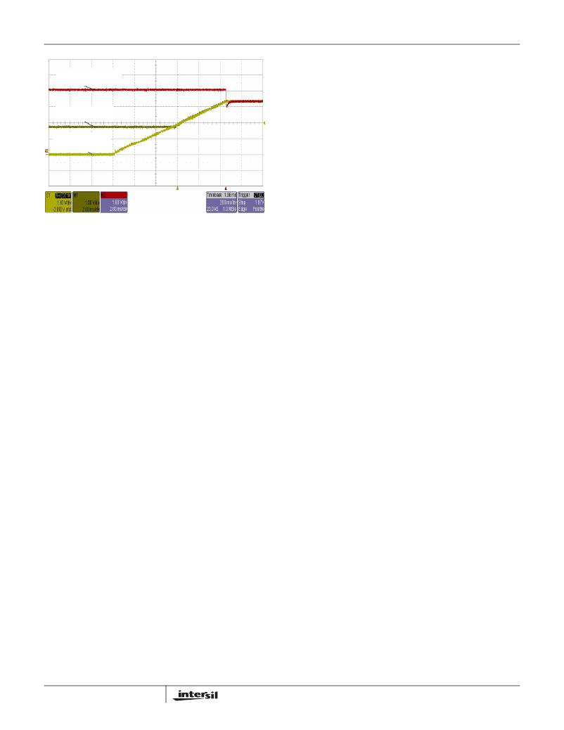
�FIGURE� 3.� SOFT-START� WITH� PRE-BIAS�
�soft-start� ramp� voltage� exceeds� the� output;� V� OUT� starts�
�seamlessly� ramping� from� there.� If� the� output� is� pre-biased� to�
�a� voltage� above� the� expected� value,� as� in� the� red� curve,�
�neither� MOSFET� will� turn� on� until� the� end� of� the� soft-start,� at�
�which� time� it� will� pull� the� output� voltage� down� to� the� final�
�value.� Any� resistive� load� connected� to� the� output� will� help�
�pull� down� the� voltage� (at� the� RC� rate� of� the� R� of� the� load� and�
�the� C� of� the� output� capacitance).�
�If� the� V� IN� for� the� synchronous� buck� converter� is� from� a�
�different� supply� that� comes� up� after� V� BIAS� ,� the� soft-start�
�would� go� through� its� cycle,� but� with� no� output� voltage� ramp.�
�When� V� IN� turns� on,� the� output� would� follow� the� ramp� of� the�
�V� IN� from� zero� up� to� the� final� expected� voltage� (at� close� to�
�100%� duty� cycle,� with� COMP/EN� pin� >4V).� If� V� IN� is� too� fast,�
�there� may� be� excessive� inrush� current� charging� the� output�
�capacitors� (only� the� beginning� of� the� ramp,� from� zero� to�
�V� OUT� matters� here).� If� this� is� not� acceptable,� then� consider�
�changing� the� sequencing� of� the� power� supplies,� or� sharing�
�the� same� supply,� or� adding� sequencing� logic� to� the�
�COMP/EN� pin� to� delay� the� soft-start� until� the� V� IN� supply� is�
�ready� (see� “Input� Voltage� Considerations”� on� page� 9).�
�If� the� IC� is� disabled� after� soft-start� (by� pulling� COMP/EN� pin�
�low),� and� then� enabled� (by� releasing� the� COMP/EN� pin),�
�then� the� full� initialization� (including� OCP� sample)� will� take�
�place.� However,� there� is� no� new� OCP� sampling� during�
�overcurrent� retries.� If� the� output� is� shorted� to� GND� during�
�soft-start,� the� OCP� will� handle� it,� as� described� in� the� next�
�section.�
�7�
�BGATE� driver� is� disabled� to� allow� an� internal� 21.5μA� current�
�source� to� develop� a� voltage� across� R� BSOC� .� The� ISL8105B�
�samples� this� voltage� (which� is� referenced� to� the� GND� pin)� at�
�the� BGATE/BSOC� pin,� and� holds� it� in� a� counter� and� DAC�
�combination.� This� sampled� voltage� is� held� internally� as� the�
�Overcurrent� Set� Point,� for� as� long� as� power� is� applied,� or�
�until� a� new� sample� is� taken� after� coming� out� of� a� shut-down.�
�The� actual� monitoring� of� the� bottom-side� MOSFET's�
�on-resistance� starts� 200ns� (nominal)� after� the� edge� of� the�
�internal� PWM� logic� signal� (that� creates� the� rising� external�
�BGATE� signal).� This� is� done� to� allow� the� gate� transition�
�noise� and� ringing� on� the� LX� pin� to� settle� out� before�
�monitoring.� The� monitoring� ends� when� the� internal� PWM�
�edge� (and� thus� BGATE)� goes� low.� The� OCP� can� be� detected�
�anywhere� within� the� above� window.�
�If� the� regulator� is� running� at� high� TGATE� duty� cycles� (around�
�87%� for� 300kHz� operation),� then� the� BGATE� pulse� width�
�may� not� be� wide� enough� for� the� OCP� to� properly� sample� the�
�r� DS(ON)� .� For� those� cases,� if� the� BGATE� is� too� narrow� (or� not�
�there� at� all)� for� 3� consecutive� pulses,� then� the� third� pulse� will�
�be� stretched� and/or� inserted� to� the� 425ns� minimum� width.�
�This� allows� for� OCP� monitoring� every� third� pulse� under� this�
�condition.� This� can� introduce� a� small� pulse-width� error� on� the�
�output� voltage,� which� will� be� corrected� on� the� next� pulse;�
�and� the� output� ripple� voltage� will� have� an� unusual� 3-clock�
�pattern,� which� may� look� like� jitter.� If� the� OCP� is� disabled� (by�
�choosing� a� too-high� value� of� R� BSOC� ,� or� no� resistor� at� all),�
�then� the� pulse� stretching� feature� is� also� disabled.� Figure� 4�
�illustrates� the� BGATE� pulse� width� stretching,� as� the� width�
�gets� smaller.�
�FN6447.2�
�April� 15,� 2010�
�相关PDF资料 |
PDF描述 |
|---|---|
| VI-B7Y-EW-F3 | CONVERTER MOD DC/DC 3.3V 66W |
| ISL8105BCRZ | IC REG CTRLR BUCK PWM VM 10-DFN |
| CAT823LTDI-GT3 | IC SUPERVISOR RESET TSOT-23-5 |
| ISL8105ACRZ | IC REG CTRLR BUCK PWM VM 10-DFN |
| ISL8105CRZ | IC REG CTRLR BUCK PWM VM 10-DFN |
相关代理商/技术参数 |
参数描述 |
|---|---|
| ISL8105BCBZ-T | 功能描述:IC REG CTRLR BUCK PWM VM 8-SOIC RoHS:是 类别:集成电路 (IC) >> PMIC - 稳压器 - DC DC 切换控制器 系列:- 标准包装:4,500 系列:PowerWise® PWM 型:控制器 输出数:1 频率 - 最大:1MHz 占空比:95% 电源电压:2.8 V ~ 5.5 V 降压:是 升压:无 回扫:无 反相:无 倍增器:无 除法器:无 Cuk:无 隔离:无 工作温度:-40°C ~ 125°C 封装/外壳:6-WDFN 裸露焊盘 包装:带卷 (TR) 配用:LM1771EVAL-ND - BOARD EVALUATION LM1771 其它名称:LM1771SSDX |
| ISL8105BCRZ | 功能描述:IC REG CTRLR BUCK PWM VM 10-DFN RoHS:是 类别:集成电路 (IC) >> PMIC - 稳压器 - DC DC 切换控制器 系列:- 产品培训模块:Lead (SnPb) Finish for COTS Obsolescence Mitigation Program 标准包装:2,500 系列:- PWM 型:电流模式 输出数:1 频率 - 最大:275kHz 占空比:50% 电源电压:18 V ~ 110 V 降压:无 升压:无 回扫:无 反相:无 倍增器:无 除法器:无 Cuk:无 隔离:是 工作温度:-40°C ~ 85°C 封装/外壳:8-SOIC(0.154",3.90mm 宽) 包装:带卷 (TR) |
| ISL8105BCRZ-T | 功能描述:IC REG CTRLR BUCK PWM VM 10-DFN RoHS:是 类别:集成电路 (IC) >> PMIC - 稳压器 - DC DC 切换控制器 系列:- 标准包装:4,500 系列:PowerWise® PWM 型:控制器 输出数:1 频率 - 最大:1MHz 占空比:95% 电源电压:2.8 V ~ 5.5 V 降压:是 升压:无 回扫:无 反相:无 倍增器:无 除法器:无 Cuk:无 隔离:无 工作温度:-40°C ~ 125°C 封装/外壳:6-WDFN 裸露焊盘 包装:带卷 (TR) 配用:LM1771EVAL-ND - BOARD EVALUATION LM1771 其它名称:LM1771SSDX |
| ISL8105BEVAL1Z | 功能描述:EVAL BOARD ISL8105B RoHS:是 类别:编程器,开发系统 >> 评估板 - DC/DC 与 AC/DC(离线)SMPS 系列:- 产品培训模块:Obsolescence Mitigation Program 标准包装:1 系列:True Shutdown™ 主要目的:DC/DC,步升 输出及类型:1,非隔离 功率 - 输出:- 输出电压:- 电流 - 输出:1A 输入电压:2.5 V ~ 5.5 V 稳压器拓扑结构:升压 频率 - 开关:3MHz 板类型:完全填充 已供物品:板 已用 IC / 零件:MAX8969 |
| ISL8105BEVAL2Z | 功能描述:EVALUATION BOARD FOR ISL8105B RoHS:是 类别:编程器,开发系统 >> 评估板 - DC/DC 与 AC/DC(离线)SMPS 系列:- 产品培训模块:Obsolescence Mitigation Program 标准包装:1 系列:True Shutdown™ 主要目的:DC/DC,步升 输出及类型:1,非隔离 功率 - 输出:- 输出电压:- 电流 - 输出:1A 输入电压:2.5 V ~ 5.5 V 稳压器拓扑结构:升压 频率 - 开关:3MHz 板类型:完全填充 已供物品:板 已用 IC / 零件:MAX8969 |
发布紧急采购,3分钟左右您将得到回复。