- 您现在的位置:买卖IC网 > PDF目录15211 > ISL8105BCBZ (Intersil)IC REG CTRLR BUCK PWM VM 8-SOIC PDF资料下载
参数资料
| 型号: | ISL8105BCBZ |
| 厂商: | Intersil |
| 文件页数: | 9/16页 |
| 文件大小: | 0K |
| 描述: | IC REG CTRLR BUCK PWM VM 8-SOIC |
| 标准包装: | 980 |
| PWM 型: | 电压模式 |
| 输出数: | 1 |
| 频率 - 最大: | 330kHz |
| 占空比: | 100% |
| 电源电压: | 6.5 V ~ 14.4 V |
| 降压: | 是 |
| 升压: | 无 |
| 回扫: | 无 |
| 反相: | 无 |
| 倍增器: | 无 |
| 除法器: | 无 |
| Cuk: | 无 |
| 隔离: | 无 |
| 工作温度: | 0°C ~ 70°C |
| 封装/外壳: | 8-SOIC(0.154",3.90mm 宽) |
| 包装: | 管件 |
�� �
�
�ISL8105B�
�a� typical� power� supply� to� ramp� up� past� 6.5V� before� the�
�soft-start� ramps� begins.� This� prevents� a� disturbance� on� the�
�output,� due� to� the� internal� regulator� turning� on� or� off.� If� the�
�transition� is� slow� (not� a� step� change),� the� disturbance� should�
�V� OUT�
�be� minimal.� So� while� the� recommendation� is� to� not� have� the�
�output� enabled� during� the� transition� through� this� region,� it�
�may� be� acceptable.� The� user� should� monitor� the� output� for�
�their� application� to� see� if� there� is� any� problem.�
�t0�
�2� SOFT-START� CYCLES�
�t1�
�t2�
�The� V� IN� to� the� top-side� MOSFET� can� share� the� same� supply�
�as� V� BIAS� but� can� also� run� off� a� separate� supply� or� other�
�sources,� such� as� outputs� of� other� regulators.� If� V� BIAS�
�powers� up� first,� and� the� V� IN� is� not� present� by� the� time� the�
�initialization� is� done,� then� the� soft-start� will� not� be� able� to�
�ramp� the� output,� and� the� output� will� later� follow� part� of� the�
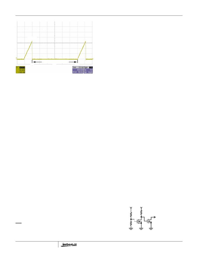
�FIGURE� 5.� OVERCURRENT� RETRY� OPERATION�
�Output� Voltage� Selection�
�The� output� voltage� can� be� programmed� to� any� level� between�
�the� 0.6V� internal� reference,� up� to� the� V� Bias� supply.� The�
�ISL8105B� can� run� at� near� 100%� duty� cycle� at� zero� load,� but�
�the� r� DS(ON)� of� the� top-side� MOSFET� will� effectively� limit� it� to�
�something� less� as� the� load� current� increases.� In� addition,� the�
�OCP� (if� enabled)� will� also� limit� the� maximum� effective� duty�
�cycle.�
�An� external� resistor� divider� is� used� to� scale� the� output�
�voltage� relative� to� the� internal� reference� voltage,� and� feed� it�
�back� to� the� inverting� input� of� the� error� amp.� See� “Typical�
��upper� resistor;� R� OFFSET� (shortened� to� R� 0� below)� is� the�
�lower� one.� The� recommended� value� for� R� 1� is� 1k� Ω� to� 5k� Ω�
�(±1%� for� accuracy)� and� then� R� OFFSET� is� chosen� according�
�to� the� equation� below.� Since� R� 1� is� part� of� the� compensation�
�circuit� (see� “Feedback� Compensation”� on� page� 11),� it� is�
�often� easier� to� change� R� OFFSET� to� change� the� output�
�voltage;� that� way� the� compensation� calculations� do� not� need�
�to� be� repeated.� If� V� OUT� =� 0.6V,� then� R� OFFSET� can� be� left�
�open.� Output� voltages� less� than� 0.6V� are� not� available.�
�V� IN� ramp� when� it� is� applied.� If� this� is� not� desired,� then�
�change� the� sequencing� of� the� supplies,� or� use� the�
�COMP/EN� pin� to� disable� V� OUT� until� both� supplies� are� ready.�
�Figure� 6� shows� a� simple� sequencer� for� this� situation.� If� V� BIAS�
�powers� up� first,� Q� 1� will� be� off,� and� R� 3� pulling� to� V� BIAS� will� turn�
�Q� 2� on,� keeping� the� ISL8105B� in� shut-down.� When� V� IN� turns�
�on,� the� resistor� divider� R� 1� and� R� 2� determines� when� Q� 1� turns�
�on,� which� will� turn� off� Q� 2� and� release� the� shut-down.� If� V� IN�
�powers� up� first,� Q� 1� will� be� on,� turning� Q� 2� off;� so� the� ISL8105B�
�will� start-up� as� soon� as� V� BIAS� comes� up.� The� V� DISABLE� trip�
�point� is� 0.4V� nominal,� so� a� wide� variety� of� NFET's� or� NPN's� or�
�even� some� logic� IC's� can� be� used� as� Q� 1� or� Q� 2� ;� but� Q� 2� must� be�
�low� leakage� when� off� (open-drain� or� open-collector)� so� as� not� to�
�interfere� with� the� COMP� output.� Q� 2� should� also� be� placed� near�
�the� COMP/EN� pin.�
�The� V� IN� range� can� be� as� low� as� ~1V� (for� V� OUT� as� low� as� the�
�0.6V� reference).� It� can� be� as� high� as� 20V� (for� V� OUT� just�
�below� V� IN� ).� There� are� some� restrictions� for� running� high� V� IN�
�voltage.�
�The� first� consideration� for� high� V� IN� is� the� maximum� BOOT�
�voltage� of� 36V.� The� V� IN� (as� seen� on� LX)� +� V� BIAS� (boot�
�voltage� -� the� diode� drop)� +� any� ringing� (or� other� transients)�
�(� R� 1� +� R� 0� )�
�V� OUT� =� 0.6V� ?� --------------------------�
�V� OUT� –� 0.6V�
�R� 0�
�R� 1� ?� 0.6V�
�R� 0� =� ----------------------------------�
�Input� Voltage� Considerations�
�The� “Typical� Application� Diagram”� on� page� 2� shows� a�
�(EQ.� 2)�
�(EQ.� 3)�
�on� the� BOOT� pin� must� be� less� than� 36V.� If� V� IN� is� 20V,� that�
�limits� V� BIAS� +� ringing� to� 16V.�
�The� second� consideration� for� high� V� IN� is� the� maximum� (BOOT�
�-� V� BIAS� )� voltage;� this� must� be� less� than� 24V.� Since� BOOT� =� V� IN�
�+� V� BIAS� +� ringing,� that� reduces� to� (V� IN� +� ringing)� must� be� <24V.�
�So� based� on� typical� circuits,� a� 20V� maximum� V� IN� is� a� good�
�starting� assumption;� the� user� should� verify� the� ringing� in� their�
�particular� application.�
�standard� configuration� where� V� BIAS� is� either� 5V� (±10%)� or�
�12V� (±20%);� in� each� case,� the� gate� drivers� use� the� V� BIAS�
�voltage� for� BGATE� and� BOOT/TGATE.� In� addition,� V� BIAS� is�
�allowed� to� work� anywhere� from� 6.5V� up� to� the� 14.4V�
�maximum.� The� V� BIAS� range� between� 5.5V� and� 6.5V� is�
�NOT� allowed� for� long-term� reliability� reasons,� but�
�transitions� through� it� to� voltages� above� 6.5V� are� acceptable.�
�V� IN�
�R� 1�
�R� 2�
�V� BIAS�
�R� 3�
�Q� 1�
�TO� COMP/EN�
�Q� 2�
�There� is� an� internal� 5V� regulator� for� bias;� it� turns� on� between�
�5.5V� and� 6.5V.� Some� of� the� delay� after� POR� is� there� to� allow�
�9�
�FIGURE� 6.� SEQUENCER� CIRCUIT�
�FN6447.2�
�April� 15,� 2010�
�相关PDF资料 |
PDF描述 |
|---|---|
| VI-B7Y-EW-F3 | CONVERTER MOD DC/DC 3.3V 66W |
| ISL8105BCRZ | IC REG CTRLR BUCK PWM VM 10-DFN |
| CAT823LTDI-GT3 | IC SUPERVISOR RESET TSOT-23-5 |
| ISL8105ACRZ | IC REG CTRLR BUCK PWM VM 10-DFN |
| ISL8105CRZ | IC REG CTRLR BUCK PWM VM 10-DFN |
相关代理商/技术参数 |
参数描述 |
|---|---|
| ISL8105BCBZ-T | 功能描述:IC REG CTRLR BUCK PWM VM 8-SOIC RoHS:是 类别:集成电路 (IC) >> PMIC - 稳压器 - DC DC 切换控制器 系列:- 标准包装:4,500 系列:PowerWise® PWM 型:控制器 输出数:1 频率 - 最大:1MHz 占空比:95% 电源电压:2.8 V ~ 5.5 V 降压:是 升压:无 回扫:无 反相:无 倍增器:无 除法器:无 Cuk:无 隔离:无 工作温度:-40°C ~ 125°C 封装/外壳:6-WDFN 裸露焊盘 包装:带卷 (TR) 配用:LM1771EVAL-ND - BOARD EVALUATION LM1771 其它名称:LM1771SSDX |
| ISL8105BCRZ | 功能描述:IC REG CTRLR BUCK PWM VM 10-DFN RoHS:是 类别:集成电路 (IC) >> PMIC - 稳压器 - DC DC 切换控制器 系列:- 产品培训模块:Lead (SnPb) Finish for COTS Obsolescence Mitigation Program 标准包装:2,500 系列:- PWM 型:电流模式 输出数:1 频率 - 最大:275kHz 占空比:50% 电源电压:18 V ~ 110 V 降压:无 升压:无 回扫:无 反相:无 倍增器:无 除法器:无 Cuk:无 隔离:是 工作温度:-40°C ~ 85°C 封装/外壳:8-SOIC(0.154",3.90mm 宽) 包装:带卷 (TR) |
| ISL8105BCRZ-T | 功能描述:IC REG CTRLR BUCK PWM VM 10-DFN RoHS:是 类别:集成电路 (IC) >> PMIC - 稳压器 - DC DC 切换控制器 系列:- 标准包装:4,500 系列:PowerWise® PWM 型:控制器 输出数:1 频率 - 最大:1MHz 占空比:95% 电源电压:2.8 V ~ 5.5 V 降压:是 升压:无 回扫:无 反相:无 倍增器:无 除法器:无 Cuk:无 隔离:无 工作温度:-40°C ~ 125°C 封装/外壳:6-WDFN 裸露焊盘 包装:带卷 (TR) 配用:LM1771EVAL-ND - BOARD EVALUATION LM1771 其它名称:LM1771SSDX |
| ISL8105BEVAL1Z | 功能描述:EVAL BOARD ISL8105B RoHS:是 类别:编程器,开发系统 >> 评估板 - DC/DC 与 AC/DC(离线)SMPS 系列:- 产品培训模块:Obsolescence Mitigation Program 标准包装:1 系列:True Shutdown™ 主要目的:DC/DC,步升 输出及类型:1,非隔离 功率 - 输出:- 输出电压:- 电流 - 输出:1A 输入电压:2.5 V ~ 5.5 V 稳压器拓扑结构:升压 频率 - 开关:3MHz 板类型:完全填充 已供物品:板 已用 IC / 零件:MAX8969 |
| ISL8105BEVAL2Z | 功能描述:EVALUATION BOARD FOR ISL8105B RoHS:是 类别:编程器,开发系统 >> 评估板 - DC/DC 与 AC/DC(离线)SMPS 系列:- 产品培训模块:Obsolescence Mitigation Program 标准包装:1 系列:True Shutdown™ 主要目的:DC/DC,步升 输出及类型:1,非隔离 功率 - 输出:- 输出电压:- 电流 - 输出:1A 输入电压:2.5 V ~ 5.5 V 稳压器拓扑结构:升压 频率 - 开关:3MHz 板类型:完全填充 已供物品:板 已用 IC / 零件:MAX8969 |
发布紧急采购,3分钟左右您将得到回复。