- 您现在的位置:买卖IC网 > PDF目录15524 > ISL8118IRZ (Intersil)IC REG CTRLR BUCK PWM VM 28-QFN PDF资料下载
参数资料
| 型号: | ISL8118IRZ |
| 厂商: | Intersil |
| 文件页数: | 17/20页 |
| 文件大小: | 0K |
| 描述: | IC REG CTRLR BUCK PWM VM 28-QFN |
| 标准包装: | 60 |
| PWM 型: | 电压模式 |
| 输出数: | 1 |
| 频率 - 最大: | 2MHz |
| 占空比: | 100% |
| 电源电压: | 2.97 V ~ 22 V |
| 降压: | 是 |
| 升压: | 无 |
| 回扫: | 无 |
| 反相: | 无 |
| 倍增器: | 无 |
| 除法器: | 无 |
| Cuk: | 无 |
| 隔离: | 无 |
| 工作温度: | -40°C ~ 85°C |
| 封装/外壳: | 28-VFQFN 裸露焊盘 |
| 包装: | 管件 |
| 产品目录页面: | 1244 (CN2011-ZH PDF) |
�� �
�
�ISL8118�
�A� small� capacitor,� C� SEN� in� Figure� 10,� can� be� added� to�
�filter� out� noise,� typically� C� SEN� is� chosen� so� the�
�As� before,� when� tying� VFF� to� VIN,� terms� in� the� previous�
�equations� can� be� simplified� as� follows:�
�d� MAX� ?� V� IN� 1� ?� V� IN�
�0.16� ?� V� IN�
�corresponding� time� constant� does� not� reduce� the� overall�
�phase� margin� of� the� design,� typically� this� is� 2x� to� 10x�
�switching� frequency� of� the� regulator.� As� the� ISL8118�
�------------------------------� =� ---------------------------� =� 6.25�
�V� OSC�
�(EQ.� 18)�
�(EQ.� 19)�
�F� Z1� =� -------------------------------�
�supports� 100%� duty� cycle,� d� MAX� equals� 1.� The� ISL8118�
�also� uses� feed-forward� compensation,� as� such� V� OSC� is�
�equal� to� 0.16� multiplied� by� the� voltage� at� the� VFF� pin.�
�When� tying� VFF� to� V� IN� ,� Equation� 9� simplifies� to:�
�COMPENSATION� BREAK� FREQUENCY� EQUATIONS�
�1�
�2� π� ?� R� 2� ?� C� 1�
�R� 2� =� ----------------------------------�
�F� Z2� =� -------------------------------------------------�
�F� P2� =� -------------------------------�
�F� P1� =� ---------------------------------------------�
�2� π� ?� R� 2� ?� ---------------------�
�0.16� ?� R� 1� ?� F� 0� (EQ.� 10)�
�F� LC�
�2.� Calculate� C� 1� such� that� F� Z1� is� placed� at� a� fraction� of� the� F� LC� ,�
�at� 0.1� to� 0.75� of� F� LC� (to� adjust,� change� the� 0.5� factor� to�
�desired� number).� The� higher� the� quality� factor� of� the� output�
�filter� and/or� the� higher� the� ratio� F� CE� /F� LC� ,� the� lower� the� F� Z1�
�frequency� (to� maximize� phase� boost� at� F� LC� ).�
�1�
�2� π� ?� (� R� 1� +� R� 3� )� ?� C� 3�
�1�
�2� π� ?� R� 3� ?� C� 3�
�1�
�C� 1� ?� C� 2�
�C� 1� +� C� 2�
�(EQ.� 20)�
�(EQ.� 22)�
�(EQ.� 21)�
�C� 1� =� -----------------------------------------------�
�2� π� ?� R� 2� ?� C� 1� ?� F� CE� –� 1�
�1�
�2� π� ?� R� 2� ?� 0.5� ?� F� LC�
�3.� Calculate� C� 2� such� that� F� P1� is� placed� at� F� CE� .�
�C� 1�
�C� 2� =� --------------------------------------------------------�
�(EQ.� 11)�
�(EQ.� 12)�
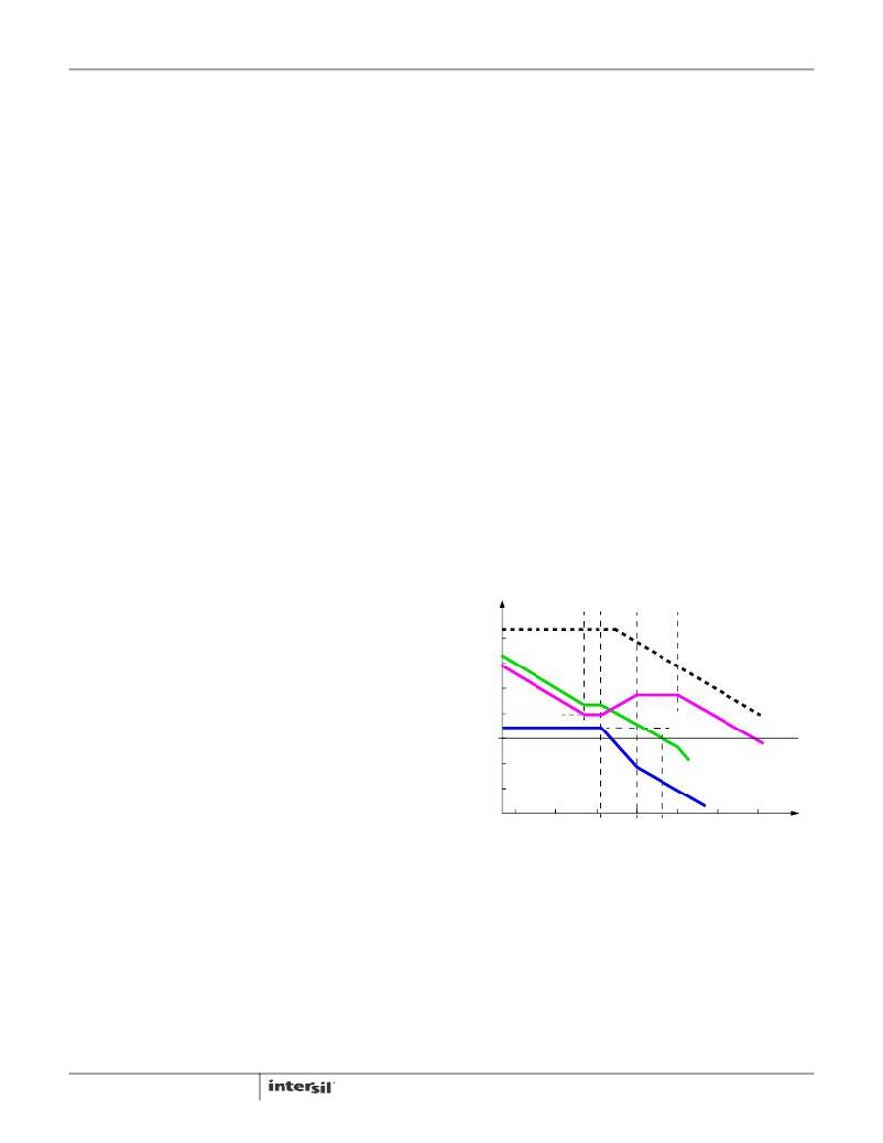
�Figure� 11� shows� an� asymptotic� plot� of� the� DC/DC� converter’s�
�gain� vs.� frequency.� The� actual� modulator� gain� has� a� high� gain�
�peak� dependent� on� the� quality� factor� (Q)� of� the� output� filter,�
�which� is� not� shown.� Using� the� above� guidelines� should� yield� a�
�compensation� gain� similar� to� the� curve� plotted.� The� open� loop�
�error� amplifier� gain� bounds� the� compensation� gain.� Check� the�
�4.� Calculate� R� 3� such� that� F� Z2� is� placed� at� F� LC� .� Calculate� C� 3�
�such� that� F� P2� is� placed� below� F� SW� (typically,� 0.5� to� 1.0�
�times� F� SW� ).� F� SW� represents� the� regulator’s� switching�
�frequency.� Change� the� numerical� factor� to� reflect� desired�
�placement� of� this� pole.� Placement� of� F� P2� lower� in� frequency�
�helps� reduce� the� gain� of� the� compensation� network� at� high�
�frequency,� in� turn� reducing� the� HF� ripple� component� at� the�
�COMP� pin� and� minimizing� resultant� duty� cycle� jitter.�
�compensation� gain� at� F� P2� against� the� capabilities� of� the� error�
�amplifier.� The� closed� loop� gain,� G� CL� ,� is� constructed� on� the� log-�
�log� graph� of� Figure� 11� by� adding� the� modulator� gain,� G� MOD�
�(in� dB),� to� the� feedback� compensation� gain,� G� FB� (in� dB).� This�
�is� equivalent� to� multiplying� the� modulator� transfer� function� and�
�the� compensation� transfer� function� and� then� plotting� the�
�resulting� gain.�
�R� 3� =� ----------------------�
�F� SW�
�R� 1�
�------------� –� 1�
�F� LC�
�(EQ.� 13)�
�F� Z1� F� Z2�
�F� P1�
�F� P2�
�MODULATOR� GAIN�
�COMPENSATION� GAIN�
�CLOSED� LOOP� GAIN�
�OPEN� LOOP� E/A� GAIN�
�C� 3� =� -------------------------------------------------�
�1�
�2� π� ?� R� 3� ?� 0.7� ?� F� SW�
�(EQ.� 14)�
�20� log� ?� --------� ?�
�OSC�
�It� is� recommended� that� a� mathematical� model� is� used� to� plot�
�the� loop� response.� Check� the� loop� gain� against� the� error�
�amplifier’s� open-loop� gain.� Verify� phase� margin� results� and�
�adjust� as� necessary.� The� following� equations� describe� the�
�frequency� response� of� the� modulator� (G� MOD� ),� feedback�
�0�
�R2�
�?� R1� ?�
�d� MAX� ?� V� IN�
�20� log� ---------------------------------�
�V�
�G� CL�
�G� FB�
�d� MAX� ?� V� IN� 1� +� s� (� f� )� ?� ESR� ?� C�
�G� MOD� (� f� )� =� ------------------------------� ?� -----------------------------------------------------------------------------------------------------------�
�compensation� (G� FB� )� and� closed-loop� response� (G� CL� ):�
�V� OSC� 1� +� s� (� f� )� ?� (� ESR� +� DCR� )� ?� C� +� s� (� f� )� ?� L� ?� C�
�LOG�
�F� LC�
�F� CE�
�F� 0�
�G� MOD�
�FREQUENCY�
�(EQ.� 15)�
�FIGURE� 11.� ASYMPTOTIC� BODE� PLOT� OF� CONVERTER� GAIN�
�G� FB� (� f� )� =� ----------------------------------------------------� ?�
�1� +� s� (� f� )� ?� (� R� 1� +� R� 3� )� ?� C� 3�
�(� 1� +� s� (� f� )� ?� R� 3� ?� C� 3� )� ?� ?� 1� +� s� (� f� )� ?� R� 2� ?� ?� ?� ?�
�?� ?� C� 1� ?� C� 2� ?� ?�
�1� +� s� (� f� )� ?� R� 2� ?� C� 1�
�s� (� f� )� ?� R� 1� ?� (� C� 1� +� C� 2� )�
�-------------------------------------------------------------------------------------------------------------------------�
�---------------------�
�?� ?� C� 1� +� C� 2� ?� ?�
�(EQ.� 16)�
�A� stable� control� loop� has� a� gain� crossing� with� close� to� a�
�-20dB/decade� slope� and� a� phase� margin� greater� than� 45°.�
�Include� worst� case� component� variations� when� determining�
�phase� margin.� The� mathematical� model� presented� makes� a�
�number� of� approximations� and� is� generally� not� accurate� at�
�frequencies� approaching� or� exceeding� half� the� switching�
�G� CL� (� f� )� =� G� MOD� (� f� )� ?� G� FB� (� f� )�
�where� ,� s� (� f� )� =� 2� π� ?� f� ?� j�
�(EQ.� 17)�
�frequency.� When� designing� compensation� networks,� select�
�target� crossover� frequencies� in� the� range� of� 10%� to� 30%� of�
�the� switching� frequency,� F� SW� .�
�17�
�FN6325.2�
�November� 29,� 2012�
�相关PDF资料 |
PDF描述 |
|---|---|
| ISL8130IRZ | IC REG CTRLR BST FLYBK PWM 20QFN |
| ADZS-BF537-ASKIT | BOARD EVAL SKIT ADSP-BF537 |
| ECC18DRAS | CONN EDGECARD 36POS R/A .100 SLD |
| V300C36C75BF | CONVERTER MOD DC/DC 36V 75W |
| SEK100M250ST | CAP ALUM 10UF 250V 20% RADIAL |
相关代理商/技术参数 |
参数描述 |
|---|---|
| ISL8118IRZ-T | 功能描述:IC REG CTRLR BUCK PWM VM 28-QFN RoHS:是 类别:集成电路 (IC) >> PMIC - 稳压器 - DC DC 切换控制器 系列:- 产品培训模块:Lead (SnPb) Finish for COTS Obsolescence Mitigation Program 标准包装:2,500 系列:- PWM 型:电流模式 输出数:1 频率 - 最大:275kHz 占空比:50% 电源电压:18 V ~ 110 V 降压:无 升压:无 回扫:无 反相:无 倍增器:无 除法器:无 Cuk:无 隔离:是 工作温度:-40°C ~ 85°C 封装/外壳:8-SOIC(0.154",3.90mm 宽) 包装:带卷 (TR) |
| ISL8120 | 制造商:INTERSIL 制造商全称:Intersil Corporation 功能描述:Dual/n-Phase Buck PWM Controller with Integrated Drivers |
| ISL8120CRZ | 功能描述:IC REG CTRLR BUCK PWM VM 32-QFN RoHS:是 类别:集成电路 (IC) >> PMIC - 稳压器 - DC DC 切换控制器 系列:- 产品培训模块:Lead (SnPb) Finish for COTS Obsolescence Mitigation Program 标准包装:2,500 系列:- PWM 型:电流模式 输出数:1 频率 - 最大:275kHz 占空比:50% 电源电压:18 V ~ 110 V 降压:无 升压:无 回扫:无 反相:无 倍增器:无 除法器:无 Cuk:无 隔离:是 工作温度:-40°C ~ 85°C 封装/外壳:8-SOIC(0.154",3.90mm 宽) 包装:带卷 (TR) |
| ISL8120CRZ-T | 功能描述:IC REG CTRLR BUCK PWM VM 32-QFN RoHS:是 类别:集成电路 (IC) >> PMIC - 稳压器 - DC DC 切换控制器 系列:- 产品培训模块:Lead (SnPb) Finish for COTS Obsolescence Mitigation Program 标准包装:2,500 系列:- PWM 型:电流模式 输出数:1 频率 - 最大:275kHz 占空比:50% 电源电压:18 V ~ 110 V 降压:无 升压:无 回扫:无 反相:无 倍增器:无 除法器:无 Cuk:无 隔离:是 工作温度:-40°C ~ 85°C 封装/外壳:8-SOIC(0.154",3.90mm 宽) 包装:带卷 (TR) |
| ISL8120CRZ-TS2568 | 制造商:Intersil Corporation 功能描述:INTEL, ISL8120CRZ-T W/BARCODE LABELS, 12 MONTH D/C RESTRICTI - Tape and Reel |
发布紧急采购,3分钟左右您将得到回复。