- 您现在的位置:买卖IC网 > PDF目录20608 > ISL8510IRZ-T (Intersil)IC REG DL BUCK/LINEAR 24-QFN PDF资料下载
参数资料
| 型号: | ISL8510IRZ-T |
| 厂商: | Intersil |
| 文件页数: | 18/21页 |
| 文件大小: | 0K |
| 描述: | IC REG DL BUCK/LINEAR 24-QFN |
| 标准包装: | 6,000 |
| 拓扑: | 降压(降压)(1),线性(LDO)(1) |
| 功能: | 任何功能 |
| 输出数: | 2 |
| 频率 - 开关: | 500kHz |
| 电压/电流 - 输出 1: | 0.6 V ~ 20 V,1A |
| 电压/电流 - 输出 2: | 0.6 V ~ 4.2 V,500mA |
| 带 LED 驱动器: | 无 |
| 带监控器: | 无 |
| 带序列发生器: | 无 |
| 电源电压: | 5V,5.5 V ~ 25 V |
| 工作温度: | -40°C ~ 85°C |
| 安装类型: | 表面贴装 |
| 封装/外壳: | 24-VFQFN 裸露焊盘 |
| 供应商设备封装: | 24-QFN(4x4) |
| 包装: | 带卷 (TR) |
�� �
�
�ISL8510�
�to� supply� the� current� needed� each� time� the� switching�
�MOSFET� turns� on.� Place� the� small� ceramic� capacitors�
�physically� close� to� the� MOSFET� VIN� pins� (switching�
�MOSFET� drain)� and� the� Schottky� diode� anode.�
�The� important� parameters� for� the� bulk� input� capacitance� are�
�the� voltage� rating� and� the� RMS� current� rating.� For� reliable�
�operation,� select� bulk� capacitors� with� voltage� and� current�
�ratings� above� the� maximum� input� voltage� and� largest� RMS�
�current� required� by� the� circuit.� Their� voltage� rating� should� be�
�at� least� 1.25x� greater� than� the� maximum� input� voltage,� while�
�a� voltage� rating� of� 1.5x� is� a� conservative� guideline.� For� most�
�cases,� the� RMS� current� rating� requirement� for� the� input�
�capacitor� of� a� buck� regulator� is� approximately� 1/2� the� DC�
�180°.� Equations� 10� through� 13� relate� the� compensation�
�network’s� poles,� zeros� and� gain� to� the� components� (R� 1� ,� R� 2� ,�
�R� 3� ,� C� 1� ,� C� 2� ,� and� C� 3� )� in� Figure� 31.� Use� these� guidelines� for�
�locating� the� poles� and� zeros� of� the� compensation� network:�
�1.� Pick� Gain� (R� 2� /R� 1� )� for� desired� converter� bandwidth.�
�2.� Place� 1st� Zero� Below� Filter’s� Double� Pole� (~75%� f� LC� ).�
�3.� Place� 2nd� Zero� at� Filter� ’s� Double� Pole.�
�4.� Place� 1st� Pole� at� the� ESR� Zero.�
�5.� Place� 2nd� Pole� at� Half� the� Switching� Frequency.�
�6.� Check� Gain� against� Error� Amplifier� ’s� Open-Loop� Gain.�
�7.� Estimate� Phase� Margin� -� Repeat� if� Necessary.�
�load� current.�
�OSC�
�DRIVER�
�V� IN�
�The� maximum� RMS� current� required� by� the� regulator� may� be�
�PWM�
�COMPARATOR�
�L� O�
�V� DDQ�
�--------------� � ?� I� OUT�
�+� ------� � ?� -----------------------------� � --------------� ?� ?�
�I� RMS�
�?�
�V� IN� ?� ?�
�?�
�L� � f� s�
�V� IN�
�-�
�C� O�
�-�
�closely� approximated� through� Equation� 7:�
�V� OUT� 2� 1� V� IN� –� V� OUT� V� OUT� 2�
�=�
�MAX� MAX� 12�
�(EQ.� 7)�
�For� a� through� hole� design,� several� electrolytic� capacitors�
�may� be� needed.� For� surface� mount� designs,� solid� tantalum�
�capacitors� can� be� used,� but� caution� must� be� exercised� with�
�regard� to� the� capacitor� surge� current� rating.� These�
�Δ� V� OSC�
�+�
�Z� FB�
�V� E/A�
�+�
�ERROR�
�AMP�
�DRIVER�
�Z� IN�
�REFERENCE�
�PHASE�
�ESR�
�(PARASITIC)�
�capacitors� must� be� capable� of� handling� the� surge-current� at�
�DETAILED� COMPENSATION� COMPONENTS�
�power-up.� Some� capacitor� series� available� from� reputable�
�manufacturers� are� surge� current� tested.�
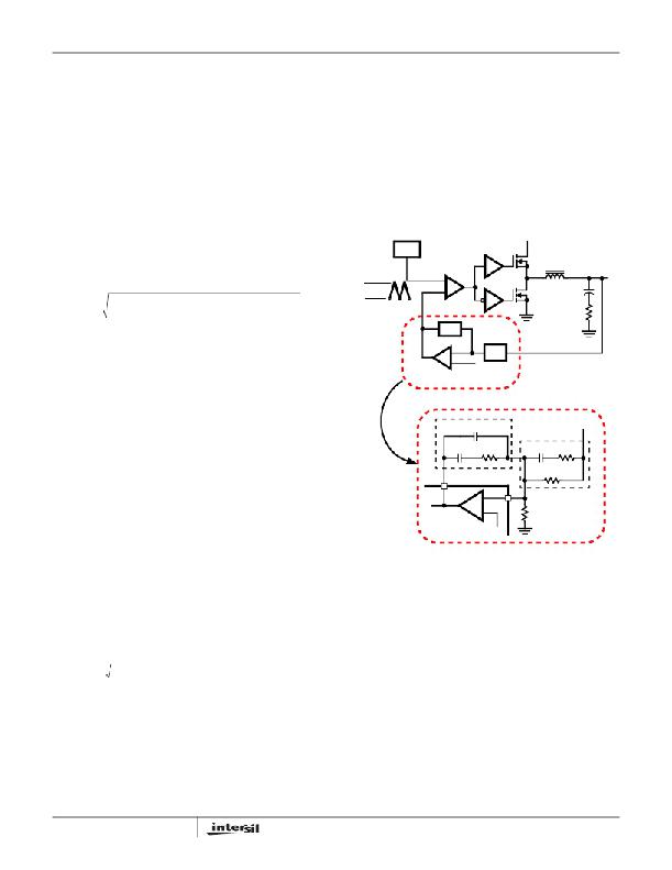
�Feedback� Compensation�
�Figure� 30� highlights� the� voltage-mode� control� loop� for� a�
�synchronous-rectified� buck� converter.� The� output� voltage�
�C� 1�
�C� 2�
�COMP�
�R� 2�
�Z� FB�
�C� 3�
�Z� IN�
�R� 1�
�R� 3�
�V� DDQ�
�(V� OUT� )� is� regulated� to� the� Reference� voltage� level.� The� error�
�amplifier� output� (V� E/A� )� is� compared� with� the� oscillator� (OSC)�
�triangular� wave� to� provide� a� pulse-width� modulated� (PWM)�
�-�
�+�
�FB�
�R� 4�
�V� DDQ� =� 0.8� � ?� 1� +� ------� 1� -� ?�
�wave� with� an� amplitude� of� V� IN� at� the� PHASE� node.� The�
�PWM� wave� is� smoothed� by� the� output� filter� (L� O� and� C� O� ).�
�The� modulator� transfer� function� is� the� small-signal� transfer�
�function� of� V� OUT� /V� E/A� .� This� function� is� dominated� by� a� DC�
�Gain� and� the� output� filter� (L� O� and� C� O� ),� with� a� double� pole�
�break� frequency� at� f� LC� and� a� zero� at� f� ESR� .� The� DC� Gain� of�
�the� modulator� is� simply� the� input� voltage� (V� IN� )� divided� by� the�
�peak-to-peak� oscillator� voltage� Δ� V� OSC� .�
�ISL8510�
�REFERENCE�
�?� R� ?�
�?� R� 4� ?�
�FIGURE� 30.� VOLTAGE-MODE� BUCK� CONVERTER�
�COMPENSATION� DESIGN� AND� OUTPUT�
�VOLTAGE� SELECTION�
�Compensation� Break� Frequency� Equations�
�F� LC� =� -------------------------------------------�
�f� Z1� =� ------------------------------------�
�F� ESR� =� --------------------------------------------�
�f� Z2� =� -------------------------------------------------------�
�Modulator� Break� Frequency� Equations�
�1�
�2� π� x� LO� x� CO�
�1�
�2� π� x� ESR� x� C� O�
�(EQ.� 8)�
�(EQ.� 9)�
�1�
�2� π� x� R� 2� x� C� 2�
�1�
�2� π� x� (� R� 1� +� R� 3� )� x� C� 3�
�(EQ.� 10)�
�(EQ.� 11)�
�f� P1� =� ---------------------------------------------------------�
�2� π� x� R� 2� x� ?� ----------------------� ?�
�f� P2� =� ------------------------------------�
�The� compensation� network� consists� of� the� error� amplifier�
�(internal� to� the� ISL6537)� and� the� impedance� networks� Z� IN�
�and� Z� FB� .� The� goal� of� the� compensation� network� is� to� provide�
�a� closed� loop� transfer� function� with� the� highest� 0dB� crossing�
�frequency� (f� 0dB� )� and� adequate� phase� margin.� Phase� margin�
�is� the� difference� between� the� closed� loop� phase� at� f� 0dB� and�
�18�
�1�
�?� C� 1� x� C� 2� ?�
�?� C� 1� +� C� 2� ?�
�1�
�2� π� x� R� 3� x� C� 3�
�(EQ.� 12)�
�(EQ.� 13)�
�FN6516.2�
�December� 15,� 2008�
�相关PDF资料 |
PDF描述 |
|---|---|
| REC3-0505SRW/H6/A | CONV DC/DC 3W 4.5-9VIN 05VOUT |
| V110C3V3H50B3 | CONVERTER MOD DC/DC 3.3V 50W |
| F951C226KQAAQ2 | CAP TANT 22UF 16V 10% 1206 |
| ISL6549CRZ-T | IC REG DL BCK/LINEAR SYNC 16-QFN |
| UH4PBC-M3/86A | DIODE 4A 100V 25NS DUAL TO277A |
相关代理商/技术参数 |
参数描述 |
|---|---|
| ISL85402EVAL1Z | 制造商:Intersil Corporation 功能描述:ISL85402 EVAL BOARD1 - 20LD QFN - INPUT VOLTAGE 36V, 2.5A - Bulk |
| ISL85402IRZ | 功能描述:IC REG BUCK BOOST SYNC ADJ 20QFN RoHS:是 类别:集成电路 (IC) >> PMIC - 稳压器 - DC DC 开关稳压器 系列:- 产品培训模块:Lead (SnPb) Finish for COTS Obsolescence Mitigation Program 标准包装:2,500 系列:- 类型:降压(降压) 输出类型:两者兼有 输出数:1 输出电压:5V,1 V ~ 10 V 输入电压:3.5 V ~ 28 V PWM 型:电流模式 频率 - 开关:220kHz ~ 1MHz 电流 - 输出:600mA 同步整流器:无 工作温度:-40°C ~ 125°C 安装类型:表面贴装 封装/外壳:16-SSOP(0.154",3.90mm 宽) 包装:带卷 (TR) 供应商设备封装:16-QSOP |
| ISL85402IRZ-T | 功能描述:IC REG BUCK BOOST SYNC ADJ 20QFN RoHS:是 类别:集成电路 (IC) >> PMIC - 稳压器 - DC DC 开关稳压器 系列:- 产品培训模块:Lead (SnPb) Finish for COTS Obsolescence Mitigation Program 标准包装:2,500 系列:- 类型:降压(降压) 输出类型:两者兼有 输出数:1 输出电压:5V,1 V ~ 10 V 输入电压:3.5 V ~ 28 V PWM 型:电流模式 频率 - 开关:220kHz ~ 1MHz 电流 - 输出:600mA 同步整流器:无 工作温度:-40°C ~ 125°C 安装类型:表面贴装 封装/外壳:16-SSOP(0.154",3.90mm 宽) 包装:带卷 (TR) 供应商设备封装:16-QSOP |
| ISL85402IRZ-T7A | 功能描述:直流/直流开关调节器 SWITCHING REG 4X4 QFN RoHS:否 制造商:International Rectifier 最大输入电压:21 V 开关频率:1.5 MHz 输出电压:0.5 V to 0.86 V 输出电流:4 A 输出端数量: 最大工作温度: 安装风格:SMD/SMT 封装 / 箱体:PQFN 4 x 5 |
| ISL85402IRZ-TK | 功能描述:IC REG BUCK BOOST SYNC ADJ 20QFN RoHS:是 类别:集成电路 (IC) >> PMIC - 稳压器 - DC DC 开关稳压器 系列:- 产品培训模块:Lead (SnPb) Finish for COTS Obsolescence Mitigation Program 标准包装:2,500 系列:- 类型:降压(降压) 输出类型:两者兼有 输出数:1 输出电压:5V,1 V ~ 10 V 输入电压:3.5 V ~ 28 V PWM 型:电流模式 频率 - 开关:220kHz ~ 1MHz 电流 - 输出:600mA 同步整流器:无 工作温度:-40°C ~ 125°C 安装类型:表面贴装 封装/外壳:16-SSOP(0.154",3.90mm 宽) 包装:带卷 (TR) 供应商设备封装:16-QSOP |
发布紧急采购,3分钟左右您将得到回复。